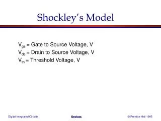
Shockley’s Model
290 likes | 566 Vues
Shockley’s Model. V gs = Gate to Source Voltage, V V ds = Drain to Source Voltage, V V tn = Threshold Voltage, V. Shockley’s Model. n = ( n ox /t ox ) (W/L) A/V 2 MOS Transistor Gain Factor n = Mobility of electrons, cm 2 /V-Sec

Shockley’s Model
E N D
Presentation Transcript
Shockley’s Model Vgs = Gate to Source Voltage, V Vds = Drain to Source Voltage, V Vtn = Threshold Voltage, V
Shockley’s Model n = (n ox/tox) (W/L) A/V2 MOS Transistor Gain Factor n = Mobility of electrons, cm2/V-Sec ox = Oxide Permittivity, F/cm, tox = Oxide thickness, cm W = Width of the transistor, microns L = Length of the transistor, microns
Shockley’s Model • The drain to source current of an nMOS device is given by Ids = 0 ; Cut-off region; Vgs<Vtn Ids = n/2 [2(Vgs – Vtn)Vds - Vds2 ] ; Linear Region; Vds < (Vgs – Vtn) Ids = n/2 (Vgs – Vtn)2; Saturation Region; Vds (Vgs – Vtn);
MOSFET Scaling • Constant Field Scaling • Constant Voltage Scaling • Lateral Scaling • SCALING - refers to ordered reduction in dimensions of the • MOSFET and other VLSI features • Reduce Size of VLSI chips. • Change operational characteristics of MOSFETs and parasitic. • Physical limits restrict degree of scaling that can be achieved.
Constant Field Scaling • The electric field E is kept constant, and the scaled device is obtained by applying a dimensionless scale-factor a (such that E is unchanged): • all dimensions, including those vertical to the surface (1/a) • device voltages (1/a) • the concentration densities (a).
Constant Voltage Scaling • Vdd is kept constant. • All dimensions, including those vertical to the surface are scaled. • Concentration densities are scaled.
Lateral Scaling • Only the gate length is scaled L = 1/a (gate-shrink). • Year Feature Size(mm) 1980 5.0 1983 3.5 1985 2.5 1987 1.75 1989 1.25 1991 1.0 1993 0.8 1995 0.6
PARAMETER SCALING MODEL Constant Constant Lateral Field Voltage Length (L) 1/a 1/a 1/a Width (W) 1/a 1/a 1 Supply Voltage (V) 1/a 1 1 Gate Oxide thickness (tox) 1/a 1/a 1 Junction depth (Xj) 1/a 1/a 1 Current (I) 1/a a a Power Dissipation (P) 1/a2a a Electric Field 1 a 1 Load Capacitance (C) 1/a 1/a 1/a Gate Delay (T) 1/a 1/a21/a2
What’s a short channel device? Short Channel Device Channel Length is of the same order as Depletion region thickness. Leff = xj
Case 3: VG positive and larger than a certain threshold voltage.
NMOS Structure • P-type substrate (“Bulk”, “Body”) • D and S heavily doped (n+) n-regions • Gate is heavily doped polysilicon (amorphous non-crystal) • Thin layer of SiO2 to insulate Gate from Substrate • A p+ region at the Silicon-Dioxide/Substrate interface (to create a positive threshold voltage)
Gate Dimensions • L = Length W = Width • During fabrication S and D “side diffuse”: Actual L is slightly less than the drawn layout L. • LD = Amount of side diffusion • LDrawn = Layout intention of L • Leff = Effective Length • Then: Leff = LDrawn - 2 LD • We shall use L but we’ll always meanLeff Typically W>>L so we shall not mention Weff Gate Oxide thickness = tox
Technology Trends • The principal thrust in MOS technology is to reduce both L and tox • Typical values (as of Year 2000):
CMOS • PMOS fabricated in a “local substrate” called “well” • All NMOS devices on a chip share the same substrate • Each PMOS device on a chip has an independent n-well
MOS Symbols • Symbols (a) are the most general, allowing B to be connected anywhere. • Symbols (b) will be used most frequently: Whenever B of NMOS is tied to GND, or B of PMOS is tied to VDD • Symbols (c) used in digital circuits.
MOS transistors Types and Symbols D D G G S S Depletion NMOS Enhancement NMOS D D G G B S S NMOS with PMOS Enhancement Bulk Contact