Download
1 / 1
10 likes | 161 Vues
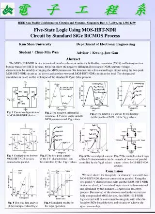
IEEE Asia Pacific Conference on Circuits and Systems , Singapore Dec. 4-7, 2006, pp. 1356-1359. Five-State Logic Using MOS-HBT-NDR Circuit by Standard SiGe BiCMOS Process. Kun Shan University. Department of Electronic Engineering. Student : Chun-Min Wen. Advisor : Kwang-Jow Gan. Abstract

E N D
IEEE Asia Pacific Conference on Circuits and Systems , Singapore Dec. 4-7, 2006, pp. 1356-1359 Five-State Logic Using MOS-HBT-NDR Circuit by Standard SiGe BiCMOS Process Kun Shan University Department of Electronic Engineering Student:Chun-Min Wen Advisor:Kwang-Jow Gan Abstract The MOS-HBT-NDR device is made of metal-oxide-semiconductor field-effect-transistor (MOS) and heterojunction bipolar transistor (HBT) devices, but it can show the negative-differential-resistance (NDR) current-voltage characteristic by suitably arranging the MOS parameters. We demonstrate a five-valued logic circuit using the two-peak MOS-HBT-NDR circuit as the driver and another two-peak MOS-HBT-NDR circuit as the load. The design and simulation is based on the technique of the standard 0.35μm SiGe process. Fig. 1 Circuit configuration of A MOS-HBT-NDR device. Fig. 2 The negative-differential-resistance I-V curve under suitable MOS parametersand Vgg values. Fig. 3 The relative I-V curves by modulating (a) the widths of MP1, (b) the Vgg values. Fig. 4 Configuration for two MOS-HBT-NDR devices connected in parallel. Fig. 5 The first peak current of the I-V characteristics can be controlled by the Vgg1 values. Fig. 6 The second peak current of the I-V characteristics can be controlled by the Vgg1 values. Fig. 7 The multiple-valued logic is made of two sets of parallel circuit of two MOS-HBT-NDR devices. Conclusion We have shown the two-peak I-V characteristics with two MOS-HBT-NDR devices connected in parallel. Using the two-peak I-V characteristics with another MOS-HBT-NDR device as a load, a five-valued logic circuit is demonstrated and simulated by the standard 0.35μm SiGe BiCMOS process. Because all of the devices used in this circuit are fully composed of MOS devices, this MOS-HBT-NDR logic circuit will be convenient to integrate with other Si-based or SiGe-based devices and circuits to achieve the system-on-a-chip. Fig. 8 The load-line analysis of the multiple-valued logic Fig. 9 Simulated results for the logic operation.