Ferroelectric Applications
Ferroelectric Applications. By. Johari Adnan School of Microelectronic Universiti Malaysia Perlis. SHORT COURSE ON FERROELECTRIC AND OPTOELECTRONIC MATERIALS FOR MICROELECTRONIC APPLICATIONS 7 & 8 May 2007. Talk outlines. Brief overview of ferroelectric BST ferroelectric thinfilms

Ferroelectric Applications
E N D
Presentation Transcript
Ferroelectric Applications By Johari Adnan School of Microelectronic Universiti Malaysia Perlis SHORT COURSE ON FERROELECTRIC AND OPTOELECTRONIC MATERIALS FOR MICROELECTRONIC APPLICATIONS 7 & 8 May 2007
Talk outlines • Brief overview of ferroelectric • BST ferroelectric thinfilms • BST sensor applications Earliest prototype
Objectives • Understand ferroelectric phenomena • Determine transduction properties of ferroelectric thinfilms • Recognize ferroelectric thinfilm sensors potentials • Look at implementation problems
An overview of ferroelectric The word ‘ferro’ is derived from the word ferrum (iron). Ferromagnetic materials exhibit magnetic hysteresis loop. Magnetization persists even when there is no magnetic field present. MR Hc
An overview of ferroelectric: continued Magnetic remanence is due to magnetic domains which are aligned. Magnetic domain Remanence magnetic field
An overview of ferroelectric: continued Under certain conditions certain materials exhibit electric hysteresis. . PR EC
An overview of ferroelectric: continued In zero electric field, they possesses spontaneous polarization. These materials are called ferroelectric materials Net spontaneous polarization Reason why certain samples do not exhibit ferroelectric properties No spontaneous polarization
How does spontaneous polarization occur in ferroelectric? The diagram below shows perovskite structure of BaTiO3 (BST). Cubic at high temperature and non-cubic below Curie temperature. In non-cubic phase Ti atom is shifted relative to the O atom and resulted in a net polarized state.
The direction of polarization may be switched by strong external electric field.
Note: after fabrication, ferroelectric material may not have net polarization characteristic since the domains may be randomized. Application of strong electric field helps align the electric domains giving the sample net spontaneous polarization.
Some definitions (related to presence of domains) • Pyroelectricity is a migration of positive and negative charge (and therefore establishment of electric polarization) to opposite ends of a crystal's polar axis as a result of a change in temperature. • The property of some materials to store a permanent electric field, by analogy with the storage of a magnetic field by ferromagnetic materials. The BaTiO3, in a perovskite structure, is used to create ferroelectrics in the lab under the imposition of a strong electric field which permanently creates electric dipoles. • Certain crystals are called piezoelectric when they exhibit a relationship between mechanical strain (tension or compression) and voltage across their surfaces. Specifically, when compressed or pulled, a piezoelectric crystal will build up alternate charges on opposite faces, thus acting like a capacitor with an applied voltage. A current, called piezoelectricity, can then be generated between the faces. On the other hand, when subjected to an external voltage, the crystal will expand or contract accordingly.
Features central to ferroelectric sensors Ferroelectric materials when subjected to temperature variation, T, electrical field, E, and stress, , will develop electrical charges, q q k1T + k2E + k3 + k4I photoelectric? pyroelectric piezoelectric ferroelectric
Focus area • Our research is on ferroelectric materials specifically BST. BST is just a small subset of ferroelectric materials. The rest of talk is specific to BST thinfilm. • Three reasons why we choose BST thinfilms • Researchers who are knowledgeable and interested in BST • Availability of fabrication facilities • Potential of BST thinfilms as sensing/storage elements
BST thinfilm structure p Silicon BST prosess Aluminium Fine wire Indium/ Silver paste
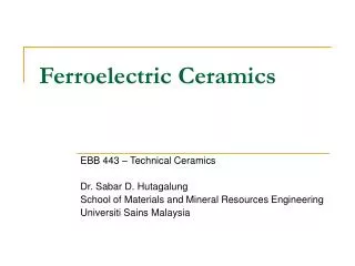
BST thinfilm 10mm x 10mm BST thinfilm
Simple BST thinfilm model from applications point of view To transduction circuit BST thinfilm
Irzaman et. al. determined from I-V measurements that BST thinfilm has diode properties The dimension of the BST thinfilm is about 8mm x 8mm At 550 Lux, the voltage across the 1M resistor is 70mV Current through the 1M is 0.07uA
Plot of voltage drop across the 1MΩ resistor versus light intensity (Lux) Voltage (mV) across 1MΩ resistor Light intensity (Lux)
Plot of resistance across BST thinfilm versus light intensity (tungsten light source) M Lux
Simple experimental setup to determine capacitance of BST thinfilm
BST thinfilm as temperature/heat sensor Peltier Type T thermocouple To DC supply To voltmeter
Plot of output voltage (mV) versus temperature (oC) voltage Temperature
Challenges in sensors development Ferroelectric materials when subjected to temperature variation, T, electrical field, E, and stress, , will develop electrical charges q q k1T + k2E + k3 • Some problems associated with sensor development • Mask unwanted contributions/modes • Suitable packaging • Right recipe tailored for a specific sensing characteristic
Fabrication technique: version 1 stripboard glass slide glue drop electrode/wire
Fabrication technique: version 3 The idea here is to focus light onto the active BST element
Immediate future plans include development of: • Gas sensors • Ultrasonic sensors • Electro-optic devices Other future plans • Integrating transduction circuits on the same sensor substrate • Active BST configurations, i.e. in the form of BJT and MOSFET • Hybrid sensor (one sensor which is capable of measuring multiple • parameters) • Other issues such as miniaturization, low power, smart, etc



![FERROELECTRIC RAM [FRAM]](https://cdn1.slideserve.com/1817127/ferroelectric-ram-fram-dt.jpg)
