MEMS-specific fabrication
MEMS-specific fabrication. Bulk micromachining Surface micromachining Deep reactive ion etching (DRIE) Other materials/processes. Bulk, Surface, DRIE. Bulk micromachining involves removing material from the silicon wafer itself Typically wet etched Traditional MEMS industry

MEMS-specific fabrication
E N D
Presentation Transcript
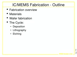
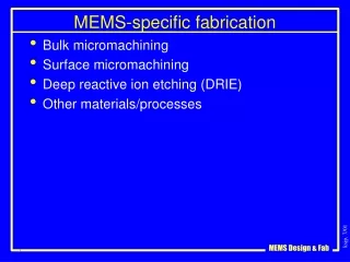
MEMS-specific fabrication • Bulk micromachining • Surface micromachining • Deep reactive ion etching (DRIE) • Other materials/processes
Bulk, Surface, DRIE • Bulk micromachining involves removing material from the silicon wafer itself • Typically wet etched • Traditional MEMS industry • Artistic design, inexpensive equipment • Issues with IC compatibility • Surface micromachining leaves the wafer untouched, but adds/removes additional layers above the wafer surface, First widely used in 1990s • Typically plasma etched • IC-like design philosophy, relatively expensive equipment • Different issues with IC compatibility • Deep Reactive Ion Etch (DRIE) removes substrate but looks like surface micromachining!
Bulk Micromachining • Many liquid etchants demonstrate dramatic etch rate differences in different crystal directions • <111> etch rate is slowest, <100> and <110> fastest • Fastest:slowest can be more than 400:1 • KOH, EDP, TMAH most common anisotropic silicon etchants • Isotropic silicon etchants • HNA • HF, nitric, and acetic acids • Lots of neat features, tough to work with • XeF2, BrF3 • gas phase, gentle • Xactix, STS selling research & production equipment
KOH Etching • Etches PR and Aluminum instantly • Masks: • SiO2 • compressive • SixNy • tensile • Parylene! • Au?
Crystal Planes & Miller Indices • [abc] in a cubic crystal is just a direction vector • (abc) is any plane perpendicular to the [abc] vector • (…)/[…] indicate a specific plane/direction • {…}/<…> indicate equivalent planes/direction Angles between directions can be determined by scalar product: the angle between [abc] and [xyz] is given by ax+by+cz = |(a,b,c)|*|(x,y,z)|*cos(theta) e.g.:
Miller indices [001] [abc] c [010] a b [100]
[001] [abc] (abc) 1/c c [010] b 1/b a 1/a [100]
{100} (001) (010) [001] [010] [100] (100)
[001] [010] (111) (110) [100]
<111> <100> Typical 100 wafer Cross-section in (110) plane The wafer flat is oriented in the [110] direction
<111> <100> (110) (111) (111) (111)
Rosette “Amplified” etch rate Masking layer Lateral undercut Un-etched silicon
Anisotropic Etching of Silicon <100> <111> 54.7 Silicon Substrate • Anisotropic etches have direction dependent etch rates in crystals • Typically the etch rates are slower perpendicularly to the crystalline planes with the highest density • Commonly used anisotropic etches in silicon include Potasium Hydroxide (KOH), Tetramethyl Ammonium Hydroxide (TmAH), and Ethylene Diamine Pyrochatecol (EDP)
Etch stops in anisotropic silicon etching • Electrochemical etch stop • High boron doping (~1e20/cm)
Micromachining Ink Jet Nozzles Microtechnology group, TU Berlin
Bulk Micromachining • Anisotropic etching allows very precise machining of silicon • Silicon also exhibit a strong piezoresistive effect • These properties, combined with silicon’s exceptional mechanical characteristics, and well-developed manufacturing base, make silicon the ideal material for precision sensors • Pressure sensors and accelerometers were the first to be developed Silicon pressure sensor chip Packaged pressure sensor
KOH etching: atomic view STM image of a (111) face with a ~10 atom step. From Weisendanger, et al., Scanning tunnelling microscopy study of Si(111)7*7 in the presence of multiple-step edges, Europhysics Letters, 12, 57 (1990).
Bulk micromachined cavities • Anisotropic KOH etch (Upperleft) • Isotropic plasma etch (upper right) • Isotropic BrF3 etch with compressive oxide still showing (lower right)
(100) (111) (111) (110) (110) (111) (110) (110) Clever KOH etching of (100) Clockwise from above: Ternez; Rosengren; Keller
Deposit sacrificial layer Pattern contacts Deposit/pattern structural layer Etch sacrificial layer Surface Micromachining
Surface micromachining material systems • Structure/ sacrificial/ etchant • Polysilicon/ Silicon dioxide/ HF • Silicon dioxide/ polysilicon/ XeF2 • Aluminum/ photoresist/ oxygen plasma • Photoresist/ aluminum/ Al etch • Aluminum/ SCS EDP, TMAH, XeF2 • Poly-SiGe poly-SiGe DI water
Residual stress gradients More tensile on top More compressive on top Just right! The bottom line: anneal poly between oxides with similar phosphorous content. ~1000C for ~60 seconds is enough.
Residual stress gradients A bad day at MCNC (1996).
Deposit first sacrificial Deposit and pattern first poly Hinges Deposit and pattern second sacrificial Pattern contacts Deposit and pattern 2nd poly Etch sacrificial
Deep Reactive Ion Etch BOSCH Patent STS, Alcatel, Trion, Oxford Instruments … Unconstrained geometry 90° side walls High aspect ratio 1:30 Easily masked (PR, SiO2) Uses high density plasma to alternatively etch silicon and deposit a etch-resistant polymer on side walls Process recipe depends on geometry Polymer Polymer deposition Silicon etch using SF6 chemistry
1 µm Scalloping and Footing issues of DRIE <100 nm silicon nanowire over >10 micron gap microgrid Footing at the bottom of device layer Milanovic et al, IEEE TED, Jan. 2001.
Typical simple SOI-MEMS Process oxide mask layer Si device layer, 20 µm thick 1) Begin with a bonded SOI wafer. Grow and etch a thin thermal oxide layer to act as a mask for the silicon etch. buried oxide layer Si handle wafer silicon 2) Etch the silicon device layer to expose the buried oxide layer. Thermal oxide 3) Etch the buried oxide layer in buffered HF to release free-standing structures.
DRIE structures • Increased capacitance for actuation and sensing • Low-stress structures • single-crystal Si only structural material • Highly stiff in vertical direction • isolation of motion to wafer plane • flat, robust structures Thermal Actuator Comb-drive Actuator 2DoF Electrostatic actuator
Sub-Micron Stereo Lithography New Micro Stereo Lithography for Freely Movable 3D Micro Structure -Super IH Process with Submicron Resolution- Koji Ikuta, Shoji Maruo, and Syunsuke Kojima Department of Micro System Engineering, school of Engineering, Nagoya University Furocho, Chikusa-ku, Nagonya 464-01, Japan Tel: +81 52 789 5024, Fax: +81 52 789 5027 E-mail: ikuta@mech.nagoya-u.ac.jp Fig. 6 Schematic diagram of the super IH process Fig. 1 Schematic diagram of IH Process Fig. 5 Process to make movable gear and shaft (a) conventional micro stereo lithography needs base layer (b) new super IH process needs no base Micro Electro Mechanical Systems Jan., 1998 Heidelberg, Germany
Sub-Micron Stereo Lithography New Micro Stereo Lithography for Freely Movable 3D Micro Structure -Super IH Process with Submicron Resolution- Koji Ikuta, Shoji Maruo, and Syunsuke Kojima Department of Micro System Engineering, school of Engineering, Nagoya University Furocho, Chikusa-ku, Nagonya 464-01, Japan Tel: +81 52 789 5024, Fax: +81 52 789 5027 E-mail: ikuta@mech.nagoya-u.ac.jp Fig. 10 Micro gear and shaft make of solidified polymer (b) side view of the gear of four teeth (d) side view of the gear of eight teeth Micro Electro Mechanical Systems Jan., 1998 Heidelberg, Germany
Combining Microstereolithography and Thick Resist UV Lithography Combining Microstereolithography and Thick Resist UV Lithography for 3D Microfabrication A. Bertsch, H. Lorenz and P. Renaud Swiss Federal Institute of Technology (EPFL) DMT – IMS, CH – 1015 Lausanne, Switzerland Tel: +41 21 693 6606 Fax: +41 693 6670 E-mail: arnaud.bertsch@epfl.ch Fig. 1 Diagram of microstereolithorgraphy apparatus using a pattern generator. Fig. 2 Influence of the geometry on the surface roughness. Micro Electro Mechanical Systems Jan., 1998 Heidelberg, Germany
Combining Microstereolithography and Thick Resist UV Lithography Combining Microstereolithography and Thick Resist UV Lithography for 3D Microfabrication A. Bertsch, H. Lorenz and P. Renaud Swiss Federal Institute of Technology (EPFL) DMT – IMS, CH – 1015 Lausanne, Switzerland Tel: +41 21 693 6606 Fax: +41 693 6670 E-mail: arnaud.bertsch@epfl.ch Fig. 5 SEM image of an object made of three imbricated springs. This structure consists of 1000 layers of 5mm each, built along the axis direction. Fig. 4 WEM photograph of a micro-turbine made by microstereolithography. Fig. 6 Enlargement of fig. 5. Micro Electro Mechanical Systems Jan., 1998 Heidelberg, Germany
Combining Microstereolithography and Thick Resist UV Lithography Combining Microstereolithography and Thick Resist UV Lithography for 3D Microfabrication A. Bertsch, H. Lorenz and P. Renaud Swiss Federal Institute of Technology (EPFL) DMT – IMS, CH – 1015 Lausanne, Switzerland Tel: +41 21 693 6606 Fax: +41 693 6670 E-mail: arnaud.bertsch@epfl.ch Fig. 15 Two level SU-8 structure with an added axle. Fig. 11 Plastic injected watch gear, total height: 1.4 mm. Micro Electro Mechanical Systems Jan., 1998 Heidelberg, Germany