Download
1 / 1
10 likes | 139 Vues
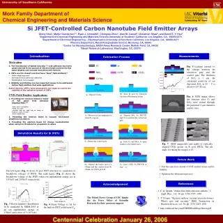
Mork Family Department of Chemical Engineering and Materials Science. Cr. P+. SiO 2. (b). Etch Si post by Electron Cyclotron Resonance etcher. (a). Deposit Cr/Au. (c). Boron was ion implanted to form P+ regions. (e). Deposit SiO 2 by PECVD and Cr to pattern the extraction gate.

E N D
Mork Family Department of Chemical Engineering and Materials Science Cr P+ SiO2 (b). Etch Si post by Electron Cyclotron Resonance etcher (a). Deposit Cr/Au (c). Boron was ion implanted to form P+ regions (e). Deposit SiO2 by PECVD and Cr to pattern the extraction gate Extraction Gate (f). Define the control gate (g). Etch Cr and SiO2 to open windows for emitter sites Control Gate N- Si substrate N+ (i). Grow CNTs by PECVD at 700 °C (h). Deposit the buffer layer Cr (40nm) and the catalyst layer Ni (20nm) for CNTs growth Si JFET-Controlled Carbon Nanotube Field Emitter Arrays Qiong Shui1, Martin Gundersen1,2, Ryan J. Umstattd3, Chongwu Zhou2, Alan M. Cassel4, lJonathan Shaw5, and David S. Y. Hsu5 1Department of Chemical Engineering and Materials Science,University of Southern California, Los Angeles, CA, 90089-0271 2Department of Electrical Engineering – Electrophysics,University of Southern California, Los Angeles, CA, 90089-0271 3Physics Department, Naval Postgraduate School, Monterey, CA, 93943 4Center for Nanotechnology, NASA Ames Research Center, Moffett Field, CA, 94035 5Naval Research Laboratory, Washington, DC, 20375 Introduction Measurements Fabrication Process • Motivation • 1. The introduction of Spindt microtip [1] cold cathodes has led to great interest in the pursuit of electron beam sources for flat panel display and vacuum microelectronic devices • 2. CNTs are the closest one that have “ideal” field emitters[2] • Stable at high temperature • Have high electrical and thermal conductivity • Exhibit ballistic electron transport. • 3. Stability and lifetime are two important issues to be addressed before field emitters find wide applications • Active devices, JFETs, were proposed in our study to control the stability of the emission current of CNTs Fig. 5 Leakage current vs. the voltage between the extraction gate and the control gate. The thickness of SiO2 is 1 m. the calculated resistivity of our deposited SiO2 at 25 °C is about 61012 Ω-cm. CNTs Field Emitter Applications 1. Providing the electron beam(s) inside of flat panel field emission displays(FED) [3] Fig. 6 SEM image shows the structure after Cr and SiO2 were etched through the patterned 2 m diameter emitter sites • lower power consumption • Wider view angles • Viewable from any angle with no change in brightness, contrast or color • Faster response time 2. Providing the electron beam in vacuum microwave amplifiers/oscillators 3. Providing the electron beam for charge neutralization when using ion thrusters for propulsion in space Simulation Results for Si JFETs Fig. 7 SEM images(left and right) of vertically aligned CNTs grown on Si post JFETs. The tilt angle for taking the images is 85 °. Future Work • Test the emission current of CNT emitter arrays and its stability • Optimize the fabrication process The left figure (Fig. 1) shows Si post JFET structure for simulation of breakdown voltages of JFETs. The right figure (Fig. 2) shows the breakdown voltage of the JFETs when ion implantation energy are at 150 keV and 200 keV, respectively References Acknowledgement 1. C. A. Spindt, "A thin-film field-emission cathode," J. Appl. Phys., vol. 39, pp. 3504-3505, 1968. 2. T. Utsumi, "Keynote address vacuum microelectronics: What's new and exciting," IEEE Transaction on Electron Devices, vol. 38, pp. 2276-2283, 1991. 3. http://other.nrl.navy.mil/CREBWorkShop/Jensen.pdf The Pulsed Power Group of USC thanks the Air Force Office of Scientific Research for their generous support. Fig. 3Boron impurity distribution in Si simulated by SRIM-2003 at an ion implantation energy of 150keV and a dose of 51015/cm3. Fig. 4 Drain Voltage vs. Id for the built-in JFET at different Vgs.