Modern IC Fabrication Technology: Doping, Oxidation, and Lithography
This lecture explores the modern IC fabrication technology, including various processes such as doping, oxidation, thin-film deposition, lithography, etch, and lithography trends. It also covers plasma processing and chemical mechanical polishing.

Modern IC Fabrication Technology: Doping, Oxidation, and Lithography
E N D
Presentation Transcript
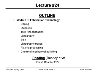
Lecture #24 OUTLINE • Modern IC Fabrication Technology • Doping • Oxidation • Thin-film deposition • Lithography • Etch • Lithography trends • Plasma processing • Chemical mechanical polishing Reading (Rabaey et al.) (Finish Chapter 2.2)
Integrated Circuit Fabrication Goal: Mass fabrication (i.e. simultaneous fabrication) of many “chips”, each a circuit (e.g. a microprocessor or memory chip) containing millions or billions of transistors Method: Lay down thin films of semiconductors, metals and insulators and pattern each layer with a process much like printing (lithography). • Materials used in a basic CMOS integrated circuit: • Si substrate – selectively doped in various regions • SiO2 insulator • Polycrystalline silicon – used for the gate electrodes • Metal contacts and wiring
Si Substrates (Wafers) Crystals are grown from a melt in boules (cylinders) with specified dopant concentrations. They are ground perfectly round and oriented (a “flat” or “notch” is ground along the boule) and then sliced like baloney into wafers. The wafers are then polished. 300 mm “notch” indicates crystal orientation Typical wafer cost: $50 Sizes: 150 mm, 200 mm, 300 mm diameter
Adding Dopants into Si Suppose we have a wafer of Si which is p-type and we want to change the surface to n-type. The way in which this is done is by ion implantation. Dopant ions are shot out of an “ion gun” called an ion implanter, into the surface of the wafer. Eaton HE3 High-Energy Implanter, showing the ion beam hitting the end-station Typical implant energies are in the range 1-200 keV. After the ion implantation, the wafers are heated to a high temperature (~1000oC). This “annealing” step heals the damage and causes the implanted dopant atoms to move into substitutional lattice sites.
Dopant Diffusion • The implanted depth-profile of dopant atoms is peaked. • In order to achieve a more uniform dopant profile, high-temperature annealing is used to diffuse the dopants • Dopants can also be directly introduced into the surface of a wafer by diffusion (rather than by ion implantation) from a dopant-containing ambient or doped solid source dopant atom concentration (logarithmic scale) as-implanted profile depth, x
Formation of Insulating Films • The favored insulator is pure silicon dioxide (SiO2). • A SiO2 film can be formed by one of two methods: • Oxidation of Si at high temperature in O2 or steam ambient • Deposition of a silicon dioxide film Applied Materials low-pressure chemical-vapor deposition (CVD) chamber ASM A412 batch oxidation furnace
Temperature range: 700oC to 1100oC Process: O2 or H2O diffuses through SiO2 and reacts with Si at the interface to form more SiO2 1 mm of SiO2 formed consumes ~0.5 mm of Si oxide thickness time, t Thermal Oxidation or “wet” oxidation “dry” oxidation
99 mm thick Si, with 1 mm SiO2 all around total thickness = 101 mm 101mm 99mm Example: Thermal Oxidation of Silicon Silicon wafer, 100 mm thick Thermal oxidation grows SiO2 on Si, but it consumes Si, so the wafer gets thinner. Suppose we grow 1 mm of oxide:
Note the 0.04mm step in the Si surface! SiO2 thickness = 1.02 mm SiO2 thickness = 0.1 mm Effect of Oxidation Rate Dependence on Thickness • The thermal oxidation rate slows with oxide thickness. Consider a Si wafer with a patterned oxide layer: Now suppose we grow 0.1 mm of SiO2: SiO2 thickness = 1 mm Si
Window Oxidation Local Oxidation (LOCOS) Selective Oxidation Techniques
Chemical Vapor Deposition (CVD) of SiO2 “LTO” • Temperature range: • 350oC to 450oC for silane • Process: • Precursor gases dissociate at the wafer surface to form SiO2 • No Si on the wafer surface is consumed • Film thickness is controlled by the deposition time oxide thickness time, t
Si film made up of crystallites SiO 2 Silicon wafer Chemical Vapor Deposition (CVD) of Si • Polycrystalline silicon (“poly-Si”): • Like SiO2, Si can be deposited by Chemical Vapor Deposition: • Wafer isheated to ~600oC • Silicon-containing gas (SiH4) is injected into the furnace: • SiH4 = Si + 2H2 • Properties: • sheet resistance (heavily doped, 0.5 m thick) = 20 / • can withstand high-temperature anneals major advantage
Al Al Ar+ Ar+ Al Physical Vapor Deposition (“Sputtering”) Used to deposit Al films: Negative Bias ( kV) I Highly energetic argon ions batter the surface of a metal target, knocking atoms loose, which then land on the surface of the wafer Al target Ar plasma Al film wafer Sometimes the substrate is heated, to ~300oC Gas pressure: 1 to 10 mTorr Deposition rate sputtering yield ion current
Lithography refers to the process of transferring a pattern to the surface of the wafer Equipment, materials, and processes needed: A mask (for each layer to be patterned) with the desired pattern A light-sensitive material (called photoresist) covering the wafer so as to receive the pattern A light source and method of projecting the image of the mask onto the photoresist (“printer” or “projection stepper” or “projection scanner”) A method of “developing” the photoresist, that is selectively removing it from the regions where it was exposed oxidation deposition ion implantation etching lithography Patterning the Layers Planar processing consists of a sequence of additive and subtractive steps with lateral patterning
The Photo-Lithographic Process optical mask oxidation photoresist exposure photoresist photoresist coating removal (ashing) photoresist develop acid etch process spin, rinse, dry step
A glass mask with a black/clear pattern is used to expose a wafer coated with ~1 m thick photoresist Image of mask appears here (3 dark areas, 4 light areas) Photoresist Exposure UV light Mask Lens Mask image is demagnified by nX photoresist Si wafer “10X stepper” “4X stepper” “1X stepper” Areas exposed to UV light are susceptible to chemical removal
Exposure using “Stepper” Tool field size increases with technology generation scribe line 1 2 wafer images Translational motion
photoresist Exposed areas of Developed photoresist Photoresist Development • Solutions with high pH dissolve the areas which were exposed to UV light; unexposed areas are not dissolved
Mask pattern (on glass plate) A A B B (A-A and B-B) Lithography Example • Look at cuts (cross sections) at various planes
mask pattern resist 0 0 1 1 2 2 3 3 4 4 5 5 m m [ [ m] m] x x resist after development 0 1 2 3 4 5 m [ m] x “A-A” Cross-Section The resist is exposed in the ranges 0 < x < 2 m & 3 < x < 5 m: The resist will dissolve in high pH solutions wherever it was exposed:
resist after development 0 1 2 3 4 5 m [ m] x “B-B” Cross-Section The photoresist is exposed in the ranges 0 < x < 5 m: mask pattern resist 0 1 2 3 4 5 m [ m] x
We have exposed mask pattern, and developed the resist photoresist First: pattern photoresist Si oxide etchant … photoresist is resistant. SiO 2 Next: Etch oxide etch stops on silicon (“selective etchant”) Last: strip resist only resist is attacked Pattern Transfer by Etching In order to transfer the photoresist pattern to an underlying film, we need a “subtractive” process that removes the film, ideally with minimal change in the pattern and with minimal removal of the underlying material(s) • Selective etch processes (using plasma or aqueous chemistry) have been developed for most IC materials Jargon for this entire sequence of process steps: “pattern using XX mask”
quartz plate chromium Photolithography • 2 types of photoresist: • positive tone: • portion exposed to light will be dissolved in developer solution • negative tone: • portion exposed to light will NOT be dissolved in developer solution from Atlas of IC Technologies by W. Maly
“i-line” “DUV” “EUV” Lithography Trends • Lithography determines the minimum feature size and limits the throughput that can be achieved in an IC manufacturing process. Thus, lithography research & development efforts are directed at • achieving higher resolution • shorter wavelengths 365 nm 248 nm 193 nm 13 nm • improving resist materials • higher sensitivity, for shorter exposure times (throughput target is 60 wafers/hr) • Lithography determines the minimum feature size and limits the throughput that can be achieved in an IC manufacturing process. Thus, lithography research & development efforts are directed at • achieving higher resolution • shorter wavelengths 365 nm 248 nm 193 nm 13 nm
Reactive Ion Etcher plasma wafer RF: 13.56 MHz Plasma Processing • Plasmas are used to enhance various processes: • CVD: Energy from RF electric field assists the dissociation of gaseous molecules, to allow for thin-film deposition at higher rates and/or lower temperatures. • Plasmas are used to enhance various processes: • CVD: Energy from RF electric field assists the dissociation of gaseous molecules, to allow for thin-film deposition at higher rates and/or lower temperatures. • Etch: Ionized etchant species are more reactive and can be accelerated toward wafer (biased at negative DC potential), to provide directional etching for more precise transfer of lithographically defined features.
Dry Etching vs. Wet Etching from Atlas of IC Technologies by W. Maly • better etch selectivity • better control of etched feature sizes
Rapid Thermal Annealing (RTA) Sub-micron MOSFETs need ultra-shallow junctions (xj<50 nm) Dopant diffusion during “activation” anneal must be minimized • Short annealing time (<1 min.) at high temperature is required • Ordinary furnaces (e.g. used for thermal oxidation and CVD) heat and cool wafers at a slow rate (<50oC per minute) • Special annealing tools have been developed to enable much faster temperature ramping, and precise control of annealing time • ramp rates as fast as 200oC/second • anneal times as short as 0.5 second • typically single-wafer process chamber:
IC with 5 layers of Al wiring Oxide Isolation of Transistors p+ p+ n+ n+ SiO2 n p p Chemical Mechanical Polishing (CMP) • Chemical mechanical polishing is used to planarize the surface of a wafer at various steps in the process of fabricating an integrated circuit. • interlevel dielectric (ILD) layers • shallow trench isolation (STI) • copper metallization “damascene” process
(1) courtesy of Sung Gyu Pyo, Hynix Semiconductor (4) (2) (3) (5) Copper Metallization “Dual Damascene Process” (IBM Corporation)
CMP Tool • Wafer is polished using a slurry containing • silica particles (10-90nm particle size) • chemical etchants (e.g. HF)

