Download
1 / 40
400 likes | 561 Vues
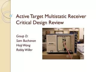
Active Target Multistatic Receiver Preliminary Design Review. Group D: Sam Buchanan Haiji Wang Robby Willer. System analysis. ATMR calibration mode diagram (Level 0). System analysis. ATMR bistatic receiver mode diagram (Level 0). System analysis. ATMR system diagram (Level 1).

E N D
Active Target MultistaticReceiverPreliminary Design Review Group D: Sam Buchanan Haiji Wang Robby Willer
System analysis ATMR calibration mode diagram (Level 0)
System analysis ATMR bistatic receiver mode diagram (Level 0)
System analysis ATMR system diagram (Level 1)
System analysis ATMR system diagram (Level 2)
Interface Definitions • RF section to DSP section • Receive chain output • Connection: SMA female/SMA female • Input magnitude: 2 Vpp (10 dBm) max • Desired SNR: ≥ 40 dB relative to thermal noise floor • Receiver card • Connection: PXIe to NI PXIe-1071 chassis backplane
Interface Definitions • DSP section to RF section • T/R switch driver (part no. TBD) and power amplifier enable (same line) • Connection: NI5772 PFI HDMI to soldered • Logic: 3.3 V LVCMOS • Zout: 50 Ω ± 20% • Transmit antenna polarization switch (part no. TBD) • Connection: NI5772 PFI HDMI to soldered • Logic: 3.3 V LVCMOS • Zout = 50 Ω ± 20% • Receiver digital attenuator control • Connection: 3 NI PXIe-1071 backplane DIO lines to receiver card DIO lines • Logic: 3.3 V LVCMOS • Zout= 50 Ω ± 20% • Waveform generator trigger • Connection: SMA female to SMA female • Logic • VIL = 0.8 V • VIH = 2 V • VOL = 0.7 V • VOH = 2.3 V • Zout: 50 Ω
Interface Definitions • DSP section • NI 5772 digitizer to 7962R FPGA card • Connection: NI FlexRIO • NI 7962R FPGA card to chassis • Connection: PXIe to chassis backplane • Controller to external HDD • Connection: SATA • P2P memory sharing b/w controller and FPGA • Connection: Chassis backplane data bus
Interface Definitions • Clock synthesizer to DSP section • Frequency synthesizer board clock signal output • Connection: SMA to SMA • Frequency range: 400 MHz to 800 MHz, 750 MHz nominal • Input power range: 2 dBm (800 mVpp) to 16 dBm (4 Vpp), 10 dBm nominal • Input jitter TBD, calculate impact on ENoB of ADC (quantization SNR) • Clock card • Connection: PXIeto chassis backplane
Etc. Specifications • Packaging: Handled by CReSIS staff • Power supply: Handled by CReSIS staff
RF Specifications • Waveform • Linear frequency modulated (LFM) signal, 150 MHz – 600 MHz (450 MHz bandwidth) • Receive chain • Construction: Two receive chains for H/V polarization; embedded on PXIe card inserted in PXIe-1071 chassis for backplane communication • Operational frequencies: 150 MHz – 600 MHz • Bandwidth: 450 MHz • Gain: 0-50 dB • Noise figure: < 2 dB • Transmit chain • Construction: External to PXIe-1071 chassis • Operational frequencies: 150 MHz – 600 MHz • Bandwidth: 450 MHz • Gain: 60 dB • Transmit power: > 100 W • Antenna • Designed by CReSIS staff • Operational frequencies: 150 MHz – 600 MHz with return loss < 10 dB • Gain: 2 dBi to 5 dBi • Power handling: > 100 W peak and > 20 W average • Dual polarized, HV isolation > 25 dB • Compact and rigid design (e.g. planar mounted bow tie) • Temperature range: -40 C to +55 C
RF Testing and Evaluation • Once parts have arrived, use lab equipment to verify cutoff frequencies of filters, insertion loss of passive components, and gain of amplifiers • Anticipate response of full chains based upon these measurements and compare with measured performance of full chains after assembly
DSP Design - Schematics FPGA application functional decomposition
DSP Design - Analysis Analog frequency representation of input sampled at 1.5 GHz
DSP Design - Analysis Digital frequency representation of input
DSP Design - Analysis multiplied input
DSP Design - Analysis Input signal after down conversion and low pass filtering
DSP Design - Analysis Input signal after down conversion, low pass filtering, and decimation
DSP Design - Analysis • Next step: matched filtering • Final step: delay system to send input to DMA FIFO if [Match Found] = true
DSP Design - Schematics Host software application functional decomposition
DSP Design - Analysis • Other design concerns • Parallelization • Data enters each FPGA at a rate of 750 MHz; FPGA can only clock up to 450 MHz • Xilinx FIR compiler supports multiple parallel input channels • FPGA to host data transfer • Testing shows 256 MB host buffer, 8 MB DMA buffer, 4 MB reads from FPGA DMA memory work • Issues with losing samples currently being investigated
DSP Test Plan • Write prototype host software with a simple FPGA application to test the NI C API, the FPGA FIFOs, and system file writing speeds • Acquire hardware, write parallelized FPGA application • Test using a 1U-DAQ to output a LFM waveform to generate a match; bypass the RF chain
Clock Specifications • GPS Oscillator • Outputs a 10 MHz clock signal, a 1 PPS signal, and status through NMEA protocol • Frequency Synthesizer • Generate a 750 MHz signal that locks to the GPS 10 MHz signal • FPGA • Captures and the GPS 1 PPS signal and generates a pulse repetition sequence (PRS) to set up the receiving parameters in the DSP section
Clock Section Test Plan • Two clock synthesizers will be fabricated, one for each GPS. Their 750 MHz outputs will be analyzed against each other to determine the phase relationship. Ideally, the two 750 MHz outputs are locked to each other. • The timing signal generation circuit will be implemented in Labview FPGA code using the 1 PPS signal from the GPS and radar parameter information from the graphical user interface. • The bistatic receiving functionality will be tested as part of the Post-integration test plan.
Post-Integration Test Plan • Anechoic chamber testing • Process data collected in MATLAB
Milestones • April 18 • Complete all individual work • Get ready for post-integration test • May 2 • Finish testing and prepare for EECS 502 open house demonstration • May 31 • Final modifications to prepare for field deployment