BG/Q Architecture
320 likes | 492 Vues
BG/Q Architecture. Scott Parker Mira Community Conference, 3/5/2013 Argonne Leadership Computing Facility Argonne National Laboratory. Argonne and the Blue Gene. 2005: Argonne accepts 1 rack (1024 nodes) of Blue Gene/L (5.6 TF) 2006: Argonne Leadership Computing Facility (ALCF) created

BG/Q Architecture
E N D
Presentation Transcript
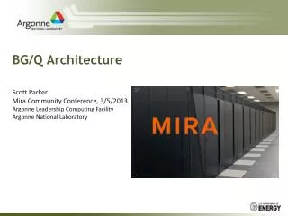
BG/Q Architecture • Scott Parker • Mira Community Conference, 3/5/2013 • Argonne Leadership Computing Facility • Argonne National Laboratory
Argonne and the Blue Gene • 2005: • Argonne accepts 1 rack (1024 nodes) of Blue Gene/L (5.6 TF) • 2006: • Argonne Leadership Computing Facility (ALCF) created • 2008: • ALCF accepts 40 racks (160k nodes) of Blue Gene/P (557 TF) • 2009: • ALCF approved for 10 petaflop system to be delivered in 2012 • 7/2012: • 48 racks of Mira Blue Gene/Q hardware delivered to ALCF • 9/2012: • 24 racks accepted • 12/2012: • full 48 racks accepted • 4/2012: • Mira in production
The Past - Intrepid • Intrepid - Blue Gene/P system • 40,960 nodes / 163,840 cores • 80 TB memory • Peak flop rate: 557 TF • Linpack flop rate: 450.3 • Challenger & Surveyor (T&D) – BG/P systems • 2,048 nodes / 8,192 cores • 4 TB of memory • Peak flop rate: 27.8 TF • Eureka – NVidia S-4 cluster • Primary use: Visualization and data analysis • 100 nodes / 800 2.0 GHz Xeon cores • 3.2 TB memory • 200 NVIDIA FX5600 GPUs • Peak flop rate: 100 TF • Storage – Data Direct Networks (DDN) storage arrays • 6+ PB capability, 80 GB/s bandwidth (GPFS and PVFS) • 14+ PB of archival storage, 10,000 volume tape archive (HPSS)
The Present - Mira • Mira – BG/Q system • 49,152 nodes / 786,432 cores • 768 TB of memory • Peak flop rate: 10 PF • Linpack flop rate: 8.1 PF • Cetus & Vesta (T&D) - BG/Q systems • 1K & 2k nodes / 32k & 64k cores • 16 TB & 32 TB of memory • 210 TF & 419 TF peak flop rate • Tukey – Nvidia system • 100 nodes / 1600 x86 cores/ 200 M2070 GPUs • 6.4 TB x86 memory / 1.2 TB GPU memory • Peak flop rate: 220 TF • Storage • Scratch: 28.8 PB raw capacity, 240 GB/s bw (GPFS) • Home: 1.8 PB raw capacity, 45 GB/s bw (GPFS) • Storage upgrade planned in 2015
ALCF BG/Q Systems (16) DDN 12Ke couplets – Scratch – 28 PB (raw), 240 GB/s Mira 48 racks/768Kcores 10 PF Infiniband Switch Complex I/O (3) DDN 12Ke couplets – Home – 1.8 PB (raw), 45 GB/s Cetus (Dev) 1 rack/16K cores 210 TF I/O Tape Library – 16 PB (raw) Tukey (Viz) 100 nodes/1600 cores 200 NVIDIA GPUs 220 TF Networks – 100Gb (via ESnet, internet2 UltraScienceNet, ) (1) DDN 12Ke – 600 TB (raw), 15 GB/s IB Switch Vesta (Dev) 2 racks/32Kcores 419 TF I/O
A brief history of the Blue Gene • In 1999 IBM began a $100 million research project to explore a novel massively parallel architecture • Initial target was protein folding applications • Design evolved out of the Cyclops64 and QCDOC architectures • First Blue Gene/L prototype appeared at #73 on the Top500 on 11/2003 • Blue Gene/L system took #1 on Top500 on 11/2004 (16 Racks at LLNL) • In 2007 the 2nd generation Blue Gene/P was introduced • In 2012 the 3rd generation Blue Gene/Q was introduced • Since being released 8 years ago,on the Top500 list: • A Blue Gene was #1 on half of the lists • On average 3 of the top 10 machines have been Blue Gene’s • The Blue Gene Q: • Currently #2 on the Top500 (LLNL, 96 racks, 20PF) • Also holds #4 (ANL), #5 (Juelich), #9 (CINECA) • #5 on the Green500
Blue Gene DNA • Leadership computing power • Leading architecture since introduction • Low speed, low power • Embedded PowerPC core with custom SIMD floating point extensions • Low frequency (L – 700 MHz, P – 850 MHz, Q – 1.6 GHz) • Massive parallelism • Many cores (L – 208k, P – 288k, Q – 1.5M) • Fast communication network(s) • Torus network (L & P – 3D, Q – 5D) • Balance: • Processor, network, and memory speeds are well balanced • Minimal system overhead • Simple lightweight OS (CNK) minimizes noise • Standard Programming Models • Fortran, C, C++, & Python languages supported • Provides MPI, OpenMP, and Pthreads parallel programming models • System on a Chip (SoC) & Custom designed ASIC • All node components on one chip, except for memory • Reduces system complexity and power, improves price / performance • High Reliability: • Sophisticated RAS (reliability, availability, and serviceability) • Dense packaging • 1024 nodes per rack
ALCF and the BG/Q Development • Over a three year period ANL collaborated with LLNL and IBM in joint research and development for the Blue Gene/Q providing input on design directions • ANL and LLNL reviewed and provided feedback on several dozen technical milestone documents related to the design of the Blue Gene/Q: • “BG/Q Design Trade-Off Study” • “BG/Q Core Choice Review” • “BG/Q Messaging Software Review” • “BG/Q Compute Node Kernel” • “API for Prefetcher” • … • Monthly conference calls to discuss BG/Q design aspects • Quarterly on-site review meetings to review status and progress • ANL & LLNL Statement-of-Work contracts specifying in detail the system specifications and deliverables • Provided representative application benchmarks • Provided IBM access to Intrepid and Mira for software development and testing at scale
C-Node n C-Node n C-Node 0 C-Node 0 CNK CNK CNK CNK Blue Gene System Architecture collective network Service Node I/O Node SystemConsole Front-endNodes FileServers Linux app app fs client optical ciod Functional Network 10Gb QDR MMCS torus Optical DB2 I/O Node Linux optical I2C app app Control Ethernet (1Gb) LoadLeveler fs client ciod FPGA JTAG
Blue Gene/Q 4. Node Card: 32 Compute Cards, Optical Modules, Link Chips; 5D Torus 3. Compute card: One chip module, 16 GB DDR3 Memory, Heat Spreader for H2O Cooling 2. Single Chip Module 1. Chip: 16+2 cores 5b. IO drawer: 8 IO cards w/16 GB 8 PCIe Gen2 x8 slots 3D I/O torus 7. System: 48 racks, 10PF/s 5a. Midplane: 16 Node Cards 6. Rack: 2 Midplanes
32 Compute Cards per Node Card Power efficient processor chips allow dense packaging Node Card contains a 2x2x2x2x2 using high bandwidth / low latency electrical interconnect Compute Node Card assembly is water-cooled Blue Gene/Q Node Card Assembly
Node has 1 BQC chip + 72 SDRAMs (16GB DDR3) Memory is soldered on for high reliability Blue Gene/Q Compute Card DRAMs (both sides) ASIC Heat spreader Assembled card
BlueGene/Q Compute Chip System-on-a-Chip design : integrates processors, memory and networking logic into a single chip • 360 mm² Cu-45 technology (SOI) • ~ 1.47 B transistors • 16 user + 1 service processors • 16 compute cores • 17th core for system functions (OS, RAS) • plus 1 redundant processor • all processors are symmetric • L1 I/D cache = 16kB/16kB • L1 prefetchengines • Crossbar switch • Connects cores via L1P to L2 slices • Aggregate read rate of 409.6 GB/s • Central shared L2 cache • 32 MB eDRAM • 16 slices • Dual memory controller • 16 GB external DDR3 memory • 42.6 GB/sbandwidth • Chip-to-chip networking • Router logic integrated into BQC chip • DMA, remote put/get, collective operations • 11 network ports • External IO • PCIe Gen2 interface
BG/Q Chip • Design based on simple, power efficient PowerPC core: • Full PowerPC compliant 64-bit CPU, PowerISAv.206 • Similar to PowerEnchip • Runs at 1.6 GHz @ 0.8V • Unique BG/Q ASIC with special features: • 4-wide SIMD floating point unit (QPX) • Transactional Memory & Speculative Execution • Fast memory based atomic operations • Stream and list based prefetching • WakeUp Unit • Universal Performance Counters
BG/Q Core • In-order execution • 4-way Simultaneous Multi-Threading • Dynamic branch prediction • 32 64 bit integer registers, 32 256 bit FP registers • Functional Units: • IU – instructions fetch and decode • XU – Branch, Integer, Load/Store instructions • AXU – Floating point instructions • Standard PowerPC instructions • QPX 4 wide SIMD • MMU – memory management (TLB) • Instruction Issue: • 2-way concurrent issue 1 XU + 1 AXU • A given thread may only issue 1 instruction per cycle • Two threads may issue 1 instruction each cycle
BG/Q Crossbar Switch X-bar L2 slice 0 Core0 L1 L1PF DRAM Controller 0 L2 slice 1 Core1 L1 L1PF DRAM Controller 1 L2 slice 15 Core16 L1 L1PF DMA • Crossbar switch connects: • L1P’s • L2 slices • Network • Other: PCIe DEVBUS interface • Aggregate bandwidth across slices: • Read: 409.6 GB/s • Write: 204.8 GB/s Network Interface
Caches • L1 Cache: • 1 per core • Data: 16KB, 8 way set associative, 64 byte line, 32 byte load/store interface, 6 cycle latency • Instruction: 16KB, 4 way set associative, 3 cycle latency • L1 Prefetcher (L1P): • 1 prefetch unit for each core • 32 entry prefetch buffer, entries are 128 bytes, 24 cycle latency • Operates in List or Stream prefetch modes • Operates as write-back buffer • L2 Cache: • Shared by all cores • Divided into 16 slices connected via crossbar switch to each core • 32 MB total, 2 MB per slice • 16 way set associative, write-back, LRU replacement, 82 cycle latency • Supports memory speculation and atomic memory operations • Serves a point of coherency, generates L1 invalidations • Has prefetch capabilities based on hints from L1P 18
L1 miss List address address L1 Prefetcher • Each core has a prefetch unit that attempts to reduce the latency for L1 misses • Prefetch buffer holds 32 128 byte cache lines • Stream Prefetching: • Default mode • Attempts to identify sequences of increasing contiguous loads based on L1 misses and prefetch data for upcoming loads • Adaptively adapts prefetch depth from 16 streams x 2 deep to 4 streams x 8 deep • List Prefetching: • 4 units per core, 1 per hardware thread • Allows prefetching of arbitrary memory access patterns accessed repeatedly • Activated by program directives bracketing sections of code • Record pattern on first loop iteration and playback for subsequent iterations • List is adaptively adjusted for missing or extra cache misses List-based “perfect” prefetching has tolerance for missing or extra cache misses
Memory • Two on chip memory controllers • Each connects to 8 L2 slices via 2 ring buses • Each controller drives a 16+2 byte DDR-3 channel at 1.33 Gb/s • Peak bandwidth is 42.67 BG/s (excluding ECC) • Latency > 350 cycles
QPX Overview • Unique 4 wide double precision SIMD instructions extending standard PowerISA with: • Full set of arithmetic functions • Load/store instructions • Permute instructions to reorganize data • 4 wide FMA instructions allow 8 flops/inst • FPU operates on: • Standard scale PowerPC FP instructions (slot 0) • 4 wide SIMD instructions • 2 wide complex arithmetic SIMD arithmetic • Standard 64 bit floating point registers are extended to 256 bits • Attached to AXU port of A2 core – A2 issues one instruction/cycle to AXU • 6 stage pipeline • 32B (256 bits) data path to/from L1 cache • Compiler can generate QPX instructions • Intrinsic functions mapping to QPX instructions allow easy QPX programming
Transactional Memory and Speculative Execution • Transactional Memory implemented in L2: • Sections of code are annotated to be executed atomically and in isolation using pragma tm_atomic • Changes from speculative threads kept separate from main memory state • Speculatively written data only available to thread writing it • At end of speculative section can revert or commit changes • Hardware identifies conflicts: read-after-write, write-after-read, write-after-write • Can store up to 30MB of speculative state • Speculative Execution implemented in L2: • Sections of code are annotated to be executed speculatively in parallel using pragmas: speculative for, speculative sections • Sequential code is partitioned into tasks which are executed speculatively in parallel • Data written by sequentially earlier threads is forwarded to later threads • Conflicts are detected by hardware at 8 bytes resolution
Fast Atomics • Provided in hardware by the L2 • 8 byte load & store operations that can alter the value at any memory address • Atomics use standard load & store instructions with special high order address bits • Allow fast synchronization and concurrent data structures – a ticket lock can by implemented to run 30x faster • Load Operations: • LoadClear, LoadIncrement, LoadDecrement, LoadIncrementBounded, LoadDecrementBounded • Store Operations: • StoreAdd, StoreAddCoherenceOnZero, StoreTwin, StoreOr, StoreXor, StoreMaxUnsigned, StoreMaxSigned • Memory for Atomics must be reserved with Kernel_L2AtomicsAllocate( )
WakeUp Unit • Each core includes a WakeUp Unit • Improves overall performance by reducing the cost of spin or polling loops • Polling threads issue instructions that occupy issues slots • Threads can configure the WakeUp unit to watch for writes to a range of memory addresses • Threads can be suspended until a watched address is written to • Thread is reactivated when watched address is written to • Improves power efficiency and resource utilization
Hardware Performance Counters • Universal Performance Counter (UPC) unit collects hardware performance events from counters on: • 17 cores • L1P’s • Wakeup Units • 16 L2 slices • Message, PCIe, and DEVBUS units • Wide range of hardware events • Network Unit maintains a separate set of counters
Inter-Processor Communication • 5D torus network: • Virtual cut-through routing with Virtual Channels to separate system and user messages • 5D torus achieves high nearest neighbor bandwidth while increasing bisectional bandwidth and reducing hops • Allows machine to be partitioned into independent sub machines. No impact from concurrently running codes. • Hardware assists for collective & barrier functions over COMM_WORLD and rectangular sub communicators • Half rack (midplane) is 4x4x4x4x2 torus • Last dimension is always 2 • No separate Collectives or Barrier network: • Single network used for point-to-point, collectives, and barrier operations • Nodes have 10 links with 2 GB/s raw bandwidth each • Bi-directional: send + receive gives 4 GB/s • 90% of bandwidth (1.8 GB/s) available to user • Additional 11th link for communication to IO nodes • Optical links between midplanes, electrical inside midplane • Hardware latency • Nearest: 80ns • Farthest: 3us (96-rack 20PF system, 31 hops) Network Performance • All-to-all: 97% of peak • Bisection: > 93% of peak • Nearest-neighbor: 98% of peak • Collective: FP reductions at 94.6% of peak • On chip per hop latency ~40 ns • Allreducehardware latency on 96k nodes ~ 6.5 us • Barrier hardware latency on 96k nodes ~ 6.3 us
Network Unit • Each chip has 11 network send units and 11 receive units: • Each can transmit and receive at 2 GB/s allows simultaneous send and receive • Total bandwidth of 44 GB/S • Total node torus bandwidth is 19x BG/L and 7.8x BG/P • 10 links used to form a 5D torus between compute nodes • 1 link used to connect to an IO node on “Bridge” nodes • 16 hardware network injection FIFOs and 16 network reception FIFOs for: user point-to-point, intra-node, high priority, collectives, and system data • Packets places in injection FIFOs are sent out via the Sender • Packets received for the node are placed in the reception FIFOs • Receivers contain 7 Virtual Channel packet buffers for: point-to-point, high priority, system, collectives • Arbitration logic routes packets from Receivers and Injection FIFOs to Senders • Collective operations are handled by Central Collective Logic • Contains performance counters: 4 per Sender, 2 per Receiver
Messaging Unit • Provides the functionality of a network interface card • Interface between the network and the BG/Q memory system, injects and pulls packets from network FIFOs • Messaging Unit is connected to node cross-bar switch with3master and 1 slave port • Supports direct puts, remote gets, and memory FIFOmessages • Maintains memory pointers to 544 injection memoryFIFOs and 272 memory reception FIFOs • Messages sent by writing descriptor into injection FIFO • Each Message Unit has 16 Injection Message Engines and 16 Reception Message Engines each tied to a network FIFO • Injection engines are assigned a descriptor, pull data and packetize • Reception engines pull data from reception FIFOs and write to in-memory FIFOs, or specified memory location • Can raise interrupts at reception memory FIFO free space threshold • Provides hardware performance counters
BG/Q IO • IO design similar to BG/L and BG/P • IO Nodes handle function shipped IO calls to parallel file system client • IO node hardware is identical to compute node hardware • IO nodes run Linux and mount file system • Compute Bridge Nodes use 1 of the 11 network links to link to IO nodes • IO nodes connect to 2 bridge nodes • IO nodes use 2 repurposed torus links for PCIe Gen2 x8 communication at 4GB/S ↔ IB/10G Ethernet ↔ file system & worl • IO nodes are not shared between compute partitions IB IB PCI_E RAID Storage & File Servers Switch BG/Q compute racks BG/Q IO
Blue Gene/Q Software High-Level Goals & Philosophy • Facilitate extreme scalability • Extremely low noise on compute nodes • High reliability: a corollary of scalability • Familiar programming modes such as MPI and OpenMP • Standards-based when possible • Open source where possible • Facilitate high performance for unique hardware: • Quad FPU, DMA unit, List-based prefetcher • TM (Transactional Memory), SE (Speculative Execution) • Wakeup-Unit, Scalable Atomic Operations • Optimize MPI and native messaging performance • Optimize libraries • Facilitate new programming models
Standards-based programming environment LinuxTM development environment Familiar GNU toolchain with glibc, pthreads, gdb Red Hat on I/O node XL Compilers C, C++, Fortran with OpenMP 3.1 Debuggers: Totalview Tools: HPC Toolkit, TAU, PAPI, Dyinst, Valgrind Message Passing Scalable MPICH2 providing MPI 2.2 with extreme message rate Efficient intermediate (PAMI) and low-level (SPI) message libraries, documented, and open source PAMI layer allows easy porting of runtimes like GA/ARMCI, Berkeley UPC, etc, Compute Node Kernel (CNK) eliminates OS noise File I/O offloaded to I/O nodes running full Linux GLIBC environment with a few restrictions for scaling Flexible and fast job control – with high availability Integrated HPC, HTC, MPMD, and sub-block jobs Noise-free partitioned networks as in previous BG New for Q Scalability Enhancements: the 17th Core RAS Event handling and interrupt off-load Event CIO Client Interface Event Application Agents: privileged application processing Wide variety of threading choices Efficient support for mixed-mode programs Support for shared memory programming paradigms Scalable atomic instructions Transactional Memory (TM) Speculative Execution (SE) Sub-blocks Integrated HTC, HPC, MPMD, Sub-blocks Integrated persistent memory High availability for service nodes with job continuation I/O nodes running Red Hat Blue Gene Q Software Innovations
