Lecture #20
OUTLINE pn Junctions (cont’d) small-signal model transient response turn-off Reading: Chapters 7, 8. Lecture #20. Small-Signal Model of the Diode. Small signal equivalent circuit:. i. +. v a. R=1/G. C. . Small-signal conductance :. Review: Charge Storage in pn-Diode.

Lecture #20
E N D
Presentation Transcript
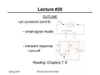
OUTLINE pn Junctions (cont’d) small-signal model transient response turn-off Reading: Chapters 7, 8 Lecture #20 EE130 Lecture 20, Slide 1
Small-Signal Model of the Diode Small signal equivalent circuit: i + va R=1/G C Small-signalconductance : EE130 Lecture 20, Slide 2
Review: Charge Storage in pn-Diode EE130 Lecture 20, Slide 3
2 types of capacitance associated with a pn junction: • CJdepletion capacitance (due to variation of depletion charge) • CDdiffusion capacitance (due to variation of stored minority charge in the quasi-neutral regions) For a one-sided p+n junction, QP >> QN so Q =QP + QN QP: EE130 Lecture 20, Slide 4
p n W conductor “insulator” conductor Depletion Capacitance What are three ways to reduce Cdep? EE130 Lecture 20, Slide 5
Total pn-Junction Capacitance i • CD dominates at moderate to high forward biases • Cdep dominates at low forward biases, reverse biases + va R=1/G EE130 Lecture 20, Slide 6
CJ-vs.-VA (Reverse Bias) EE130 Lecture 20, Slide 7
Example If the slope of the (1/Cdep)2vs.VA characteristic is -2x10²³ F-2 V-1, the intercept is 0.84V, and A is 1 mm2, find the lighter and heavier doping concentrations Nl and Nh. Solution: EE130 Lecture 20, Slide 8
Summary: Small Signal Model Depletion capacitance Conductance Diffusion capacitance EE130 Lecture 20, Slide 9
Transient Response of pn Diode • Suppose a pn-diode is forward biased, then suddenly turned off at time t = 0. Because of CD, the voltage across the pn junction depletion region cannot be changed instantaneously. The delay in switching between the ON and OFF states is due to the time required to change the amount of excess minority carriers stored in the quasi-neutral regions. EE130 Lecture 20, Slide 10
Turn-Off Transient • In order to turn the diode off, the excess minority carriers must be removed by net carrier flow out of the quasi-neutral regions and/or recombination • Carrier flow is limited by the switching circuitry EE130 Lecture 20, Slide 11
Decay of Stored Charge Consider a p+n diode (Qp >> Qn): Dpn(x) i(t) ts t vA(t) t For t > 0: ts EE130 Lecture 20, Slide 12
Examples (qualitative) Decrease tp Increase IF Increase IR i(t) i(t) i(t) ts ts ts t t t EE130 Lecture 20, Slide 13
Storage Delay Time ts • ts is the primary “figure of merit” used to characterize the transient response of pn junction diodes • By separation of variables and integration from t = 0+ to t = ts, noting that and making the approximation We conclude that EE130 Lecture 20, Slide 14

