Understanding Cut-off and Saturation Regions for NMOS and PMOS Transistors
This document explores the I-V characteristics and piecewise models of NMOS and PMOS transistors, detailing the cut-off, triode, and saturation (pinch-off) regions. It highlights the key conduction parameters such as threshold voltages (VTN, VTP), saturation currents (IDsat), and the effects of channel doping concentration. The text investigates important questions regarding the behavior of these FETs in different operating conditions, including the impact of high-K dielectrics on drain current and the performance comparison of NMOS in silicon versus gallium arsenide.


Understanding Cut-off and Saturation Regions for NMOS and PMOS Transistors
E N D
Presentation Transcript
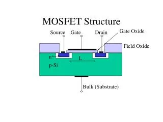
MOSFET Piecewise Models ECE 2204
Cut-off Region IG = ID= IS = 0 NMOS PMOS VGS ≤ VTN VGS≥ VTP
Nonsaturation/Triode Region IG = 0ID ≤ IDsat NMOS PMOS VGS ≥ VTN VDS ≤ VGS – VTN VGS≤ VTP VDS ≥ VGS - VTP ID= Kn[(VGS – VTN)VDS – 0.5VDS2] ID= Kp[(VGS - VTN)VDS – 0.5VDS2] RDSon= VDS/IDRDSon= VDS/ID
Saturation/Pinch-off Region IG = 0, ID = IDsat (a constant) NMOS PMOS VGS ≥ VTN VDS ≥ VDSsatVGS≤ VTPVDS≤ VDSsat VDSsat= VGS – VTNVDSsat= VGS - VTP ID= (Kn/2)(VGS – VTN)2 = (Kn/2)VDSsat2 ID= (Kp/2)(VGS - VTP)2 = (Kp/2)VDSsat2
Transition between models • NMOS enhancement mode • Cut-off and Saturation/Pinch-of • Nonsaturation/Triode and Saturation/Pinch-off • PMOS enhancement mode • Cut-off and Saturation/Pinch-of • Nonsaturation/Triode and Saturation/Pinch-off
Conduction Parameters • NMOSFET • PMOSFET where:
Questions • How does VTN or VTP change with the doping concentration of the channel? • To limit the power dissipated in a FET operating in the triode region, RDSon should be as small as possible. Should VGS be large or small? • If the oxide is changed to a high K dielectric, will ID increase or decrease? To keep the drain current unchanged, should the thickness of the oxide increase or decrease? • If you fabricated a NMOS transistor in Si and GaAs with the same doping concentrations, dimensions, and same oxide material), will ID(GasAs) be larger or smaller than ID(GasAs) when VDS = VGS – VTN?