Investigation of Photoresist Thickness Control via Spin Speed in Photolithography
110 likes | 253 Vues
This study explores the relationship between spin speed and photoresist thickness in photolithography, a vital process in semiconductor fabrication. Using Shipley 1813+ photoresist, we varied spin speeds from 3000 to 6000 RPM and measured thickness using ellipsometry and profilometry. Results showed that thickness is inversely proportional to the square root of the spin rate, evidenced by ellipsometer data aligning closely with theoretical predictions. However, profilometer readings exhibited discrepancies, possibly due to uneven coating or user interpretation errors.

Investigation of Photoresist Thickness Control via Spin Speed in Photolithography
E N D
Presentation Transcript
Photoresist Characterization Spin Speed vs. Thickness Nate Hamm, Steve Kelly, Brian MacFarland, John Yarbrough, Jeff Flint
Introduction • Photolithography is an important procedure in semiconductor processing • For our processes in the lab, having the proper thickness coating is essential • This is controlled by the spin speed on the spin coater
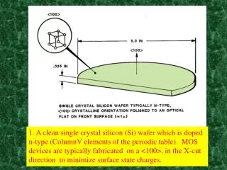
Procedure • To determine the spin speed vs. thickness, we used Shipley 1813+ photoresist and spun it on with varying dwell speeds: 3000 rpm 5000 rpm 3500 rpm 5500 rpm 4500 rpm 6000 rpm
Analysis • Once the resist was spun on, we took thickness measurements with the ellipsometer and profilometer • On the ellipsometer we used two angle measurements to obtain the correct thickness • For the profilometer we first put a glass slide over part of the resist and used the RIE to etch the exposed region
Thickness vs. Spin Speed • With the ellipsometer, we took a series of measurements across the samples as shown • This demonstrates the resist uniformity across the sample vs. spin rate
Thickness vs. Spin Speed (cont.) • Then portrayed against theoretical data, the experimental set looks accurate
Etch rate on RIE • To make measurements on the profilometer, we placed a slide over part of the photoresist and etched away the exposed portion with an oxygen plasma • Summarized in this figure are our findings on etch rate vs duration at 125 W
Profilometer Mishap? • The data we gathered from the profilometer is not close to the theoretical set
Profilometer Mishap? (cont.) • Possible reasons for the error were • Outside of optimal spin range • Uneven coating of the wafer by the photoresist • User error interpreting the data obtained by the profilometer • RIE etching process • Gnomes?
Conclusions • The ellipsometer data shows a good agreement with the Shipley data for the thickness as a function of spin rate • The thickness was shown to be inversely proportional to the square root of the spin rate • The profilometer data did not agree well with either the ellipsometer data or the Shipley data, especially at low spin speeds • This may have been a result of uneven coating of the wafer by the photoresist or outside the optimal range
Conclusions (cont.) • The etch depth vs. etch time displayed a linear relationship. • From this we found the etch rate for an oxygen plasma in the reactive ion etcher at 125 W to be 37.90Å/sec