Chap 3
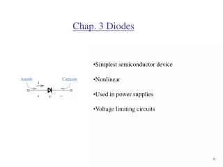
Chap 3. Simple Diode I-V Representation. V ON = 0.7v. Ideal. R Leak. R ON =ohms. Lab Diode Symbols and Ckt Representation. Diode Symbols and Ckt Representation. Diode SPICE parameters. Simple Diode Rectifer. R Leak. R on =RS =10 ohms. Limiters/Clippers. R Leak. 10V. -8V.

Chap 3
E N D
Presentation Transcript
Simple Diode I-V Representation VON = 0.7v Ideal RLeak RON =ohms
Simple Diode Rectifer RLeak Ron =RS =10 ohms
Limiters/Clippers RLeak 10V -8V
Limiters/Clippers Con’t Zeners V+VZ VZ -VD -V-VZ VD 3.3V -VD 3.3V+VZ Vo = RDiode Vin/(RDiode+R)
COMPUTATION AND THE DIODE Temperature measurement Take away!
RFID Doublers |RS + jXCB | < |20xRL + JXCL| “Short Ckt”
Zener Regulation Supplemental Material
Full Wave Rectifier Supplemental Material
Full Wave Rectifier Inputs
Basic Semiconductor Concepts-Review Fixed carrier concentration! @ Temp
Doping Example Fixed carrier concentration! Either holes or electrons
Open Ckt pn Junction Cap. Source of Junction Cap
Diode Switching Supplemental Material
Small Signal vs Large Signal Supplemental Material
DC vs AC (Small signal) Supplemental Material
Diode Summary Forward bias: Initially Qp is zero,all If goes to dQp/dt In steady state , Supplemental Material Charge Storage: The process of excess charge removal to undo the charge just built up. Until the removal of Qp is complete, diode will continue to remain on with Vd 0.7V.
Diode Summary Cuttoff: During this transient no substantial amount of excess holes is built up. id = dQj/dt. The applied current goes to charge Cj .A simple first order circuit. Charging of Cj is confirmed by the spike in the current. Supplemental Material
Diode Summary Neagtive Ir should confirm Charge at time t is given by Supplemental Material
Diode Summary Reverse recovery: All of Qp has been swept , and the diode is back at the edge of conduction. Retraces its initial turn on transient , but in reverse direction. Id is negative , but is still governed by Supplemental Material