Digital Camera Trigger Status
Digital Camera Trigger Status. May 2013 K.-H. Sulanke DESY. Three New Boards Developed. Digital Trigger Backplane. L0 Testboard. L0 Mezzanine. 9/23/2014. K.-H. Sulanke, DESY. 2. Digital Trigger L0 Mezzanine Board. Schematic simulated, very low noise preamplifier

Digital Camera Trigger Status
E N D
Presentation Transcript
Digital Camera TriggerStatus May 2013 K.-H. Sulanke DESY K.-H. Sulanke, DESY
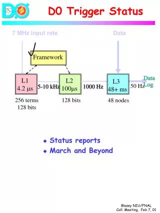
Three New Boards Developed Digital Trigger Backplane L0 Testboard L0 Mezzanine 9/23/2014 K.-H. Sulanke, DESY 2
Digital Trigger L0 Mezzanine Board Schematic simulated, very low noise preamplifier Two PCBs, a DRAGON - and a NECTAR - version 6 + 6 L0 boards assembled First test results expected next week Digital L0 Mezzanine Comp Opamp LVDS DAC Diff. Analog in LVDS out Preamp LVDS Comparator Trigger threshold 9/23/2014 K.-H. Sulanke, DESY 3
Digital Trigger L0 Mezzanine Board 6 layer PCB with length-tuned signal lines Preamplifier Comparator Trigger- Treshold-DAC 9/23/2014 K.-H. Sulanke, DESY 4
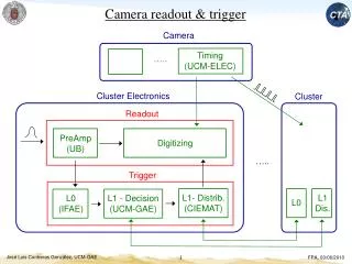
Digital Trigger L0 Test Board Testing the L0 boards AND the FE-board interface of the Dig. Trigger Backplane Xilinx with RS232 / RS485 interface, to set the discriminator thresholds etc. Dig.Trigger-Bpl. 6x5 L0 by surr. clusters L0-Testboard Single ended to diff. Digital L0 Mezzanine FPGA PMT or Pulse-Gen. Comp 7 L0 Opamp Opamp LVDS FPGA DAC FE-board interface RS-232 9/23/2014 K.-H. Sulanke, DESY 5
Digital Trigger L0 Test Board, cont. 120 mm x 260 mm, 6 Layer PCB, various analog and digital test points DESY workshop delivered the first assembled board last Friday RS232 / 485 interface FE-board Interface Connector Preamps L0-Mezzanine Test Points Xilinx Analog Inputs (Lemo) 9/23/2014 K.-H. Sulanke, DESY 6
The Digital Trigger Backplane Rev. 2 FE-board interface, compliant to FE_BP_interface_v6.doc by Gustavo M. RJ-45 ethernet Frontend board connector ethernet power CLK PPS L0_trigger trigger IP_addr HV_ena SPI / JTAG calib_cyc reserved 24V power vreg clock (opt.+power) PPS L1_trigger_out L2_trigger_in flash osc RJ-45 Xilinx FPGA flash L0 in /out and ... connectors to neighbor clusters 9/23/2014 K.-H. Sulanke, DESY 7
Digital Trigger Backplane, 8 Layer PCB PCB design by Carola Rueger DESY 9/23/2014 K.-H. Sulanke, DESY 8
Digital Trigger Backplane, cont. Test Port Xilinx JTAG port Cluster-Position- ID switches FE-board Gigabit port Xilinx Spartan-6 FPGA Power_in Clock_in PPS_in L1_out L2_in 64 bit ID ROM Local Oscillator Alternative power connector Temp. sensor FE-board 24V-fuse Atmel PROM (Xilinx config.) neighbor cluster connections FE-Board connector Local synchronous DC-DC power supply 9/23/2014 K.-H. Sulanke, DESY 9
Digital Trigger Backplane, Status 3 boards (of 5 PCBs) assembled by the DESY workshop Tests : Power supply √ Xilinx configuration via JTAG or PROM √ Local and external clock √ LVDS Interface (signal integrity) to neighbor clusters √ Inverse mode (for testing), used as a 37 bit pattern generator √ Minimum (clean) signal width is 1.25 ns Combined power / clock / pps / L1_out / L2_in RJ45-connection √ Saves cabling Various trigger alghorithms (firmware), ongoing distributed schema for clock / PPS / L1 (firmware), - Temperature sensor, - FE-board interface , - 9/23/2014 K.-H. Sulanke, DESY 10
Combined Power and Clock Input 24V, clock, and PPS over a single wire pair requires a single cat5e cable per cluster only (+ gigabit ethernet cable) Current jumps of 0.8 A did not influence the (recovered) clock quality Ext_Clock_PPS Clock_recovered PPS_recovered 24V Alternative Power conn. Clock+pps Combined Power and Clock input FE-board Gigabit port 9/23/2014 K.-H. Sulanke, DESY 11
The Centralized Trigger Schema with L2 L2 also based on Xilinx-Spartan 6 FPGAs L2 is a crate, ~ 50 x 20 x 20 cm, ~ 11 kg 18 x CSB (Cluster Service Board) 1 x L2CB (L2 Controller Board) Ethernet interface Optical / electrical camera trigger output L2 DTB 24V (optional) L0_neighbor CSB L1 L2CB FEB 7 7 #01 L0 GPS_clock Sector_trig PMT #01 ethernet FPGA … L0_neighbor … L1 FPGA FEB FPGA #18 7 #16 7 L0 Camera_trig PMT FPGA PMT = Photomultiplier Tube FEB = Frontend Board DTB = Digital Trigger Backplane CSB = Cluster Service Board L2CB = L2 Controller Board 9/23/2014 K.-H. Sulanke, DESY 12
L2 Trigger Sectors, MST, Example 271 cluster shown (1897 pixel) Each sector comprises 14..16 clusters and is connected to a certain L2 board („CSB“) 9/23/2014 K.-H. Sulanke, DESY 13
The Cluster Service Board (CSB) vreg flash 16 x Cat5e cables RJ45 RJ45 RJ45 RJ45 RJ45 RJ45 RJ45 RJ45 RJ45 RJ45 RJ45 RJ45 RJ45 RJ45 RJ45 RJ45 Cur_mon 16 x switch Clock PPS L1_trigger L3_trigger Xilinx FPGA Or optional, including 24V 24V CLK PPS L2 L3 sdat JTAG Clock_PPS_24V GND L1_trigger L3_trigger Backplane connector 9/23/2014 K.-H. Sulanke, DESY 14
Summary The Digital Trigger Backplane supports both, a distributed and a centralized schema, for the L1 trigger, the clock and the PPS-signal Centralized trigger schema preferred by me Boards needed for a distributed schema (preferred by the analog trigger group): Digital Trigger L0 mezzanine Digital Trigger Backplane A lot of firmware writing and hardware testings needed now L2 hardware development with lower priority Single CSB sufficient for a mini camera of up to 16 clusters Design progress in time with the FE-board (Nectar, Dragon) development 9/23/2014 K.-H. Sulanke, DESY 15
Outlook Assembly of about 25 Digital Trigger Backplanes planned ( 3 x 7 plus spares) until end of July CSB prototype will be available end of September 9/23/2014 K.-H. Sulanke, DESY 16
Back Up Slides 9/23/2014 K.-H. Sulanke, DESY 17
Digital L0 through Frontend-Board FPGA Allows Frontend-board-FPGA with scaler uniform FPGA internal delay (by constraints) preferred Trigger threshold DAC control by trigger FPGA, optional Separate power island with software controllable shutdown doable Dig.Trigger-Bpl. Frontend-board 6x5 L0 by surr. clusters FPGA Digital L0 Mezzanine scaler 7 Comp L0 Opamp LVDS FPGA trigger DAC PMT Poff 9/23/2014 K.-H. Sulanke, DESY
Digital Trigger Backplane, List of Key Hardware Features • Nominal power consumption: 1.5 W • Weight : 95 g + 10 g cabling to neighbor clusters -> 28 kg for LST • Automatic neighbor cluster recognition (border zone) • Synchronous DC-DC converter (24 V to 3.0 V …) • Local clock and external clock input (any diff. > 0.1V pk-pk) • FPGA load by JTAG cable or PROM or remote (by FE board) • 6 x bidirectional L0 signal connection with neighbor cluster • Temperature sensor (allows automatic delay correction, if needed) • adjustable 8 bit cluster position ID (for unique, position-independant, firmware) • Gigabit ethernet pass through connection to FE-board • RJ 45 connector as combined power and clock input (single cat5e cable) K.-H. Sulanke, DESY
From 49 Pixel to 37 Pixel Regions • Overlap still bigenough • Saves FPGA pinsandmoney • Allowsdaisychainedschemaforclock/pps 15 f 10 62 a c 12 14 60 c e a 25 13 63 65 f d d f 76 64 24 g e e 20 71 52 75 a b c f 23 70 53 d a d 22 72 74 50 c c e a 34 73 54 e d e 35 55 33 43 f f d d 30 44 42 a e c 32 40 c a 45 f 9/23/2014 K.-H. Sulanke, DESY 20
The DTB-FPGA‘s Functionality delay delay delay delay delay delay delay FPGA FPGA FPGA FPGA FPGA FPGA FPGA Xilinx Spartan 6 FPGA fanout to surrounding clusters from center cluster pix_[0][6..0] pix*_[0][4..0] calibrate STM progr. delays from surrounding clusters 37 pixel trigger fabric to L2_trigger board pix_[1][4..0] trigger pix_[6][4..0] clock PLL 9/23/2014 DESY 21
Digital Trigger Backplane, Basic Firmware Features • 37 or 49 pixel areas, depending on the trigger / clock mode (distributed or centralized) • Minimum Trigger window is 1.25 ns • Individual L0 delay calibration in 50 ps steps K.-H. Sulanke, DESY
M12 Cat6 , Combined Power / Clock Input • Instead of RJ45, more robust • by Harting, Molex, ... To be replaced by M12 9/23/2014 K.-H. Sulanke, DESY 23