
Lecture #25
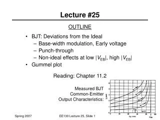
OUTLINE BJT: Deviations from the Ideal Base-width modulation, Early voltage Punch-through Non-ideal effects at low | V EB |, high | V EB | Gummel plot Reading: Chapter 11.2. Lecture #25. Measured BJT Common-Emitter Output Characteristics:. Base-Width Modulation.

Lecture #25
E N D
Presentation Transcript
OUTLINE BJT: Deviations from the Ideal Base-width modulation, Early voltage Punch-through Non-ideal effects at low |VEB|, high |VEB| Gummel plot Reading: Chapter 11.2 Lecture #25 Measured BJT Common-Emitter Output Characteristics: EE130 Lecture 25, Slide 1
Base-Width Modulation Common-Emitter Configuration, Active Mode Operation W IE IC P+ N P + VEB DpB(x) IC (VCB=0) x VEC W(VBC) 0 EE130 Lecture 25, Slide 2
The base-width modulation effect is reduced if we (a) increase the base width, W, or (b) increase the base dopant concentration, NB, or (c) decrease the collector dopant concentration, NC . Which of the above is the most acceptable action? EE130 Lecture 25, Slide 3
Early Voltage, VA Output resistance: A large VA (i.e. a large ro ) is desirable IC IB3 IB2 IB1 VEC 0 VA EE130 Lecture 25, Slide 4
Derivation of Formula for VA Output conductance: for fixed VEB where xnC is the width of the collector-junction depletion region on the base side xnC P+ N P EE130 Lecture 25, Slide 5
BJT Breakdown Mechanisms • In the common-emitter configuration, for high output voltage VCE, the output current IC will increase rapidly due to one of two mechanisms: • punch-through • avalanche EE130 Lecture 25, Slide 7
Punch-Through E-B and E-B depletion regions in the base touch, so that W = 0 As |VCB| increases, the potential barrier to hole injection decreases and therefore IC increases EE130 Lecture 25, Slide 8
Holes are injected into the base [0], then collected by the B-C junction Some holes in the B-C depletion region have enough energy to generate EHP [1] The generated electrons are swept into the base [3], then injected into the emitter [4] Each injected electron results in the injection of IEp/IEn holes from the emitter into the base [0] Avalanche Multiplication PNP BJT: • For each EHP created in the C-B depletion region by impact ionization, (IEp/IEn)+1 > bdc additional holes flow into the collector • i.e. carrier multiplication in C-B depletion region is internally amplified where VCB0 = reverse breakdown voltage of the C-B junction EE130 Lecture 25, Slide 9
Non-Ideal Effects at Low VEB • In the ideal transistor analysis, thermal R-G currents in the emitter and collector junctions were neglected. • Under active-mode operation with small VEB, the thermal recombination current is likely to be a dominant component of the base current • low emitter efficiency, hence lower gain This limits the application of the BJT for amplification at low voltages. EE130 Lecture 25, Slide 10
Non-Ideal Effects at High VEB • Decrease in bF at high IC is caused by: • high-level injection • series resistance • current crowding EE130 Lecture 25, Slide 11
Gummel Plot and bdcvs.IC high level 10 -2 injection in base I 10 -4 C bdc 10 -6 I B From top to bottom: VBC = 2V, 1V, 0V b 10 -8 excess base current due to R-G in depletion region 10 -10 10 -12 0.2 0.4 0.6 0.8 1.0 1.2 V BE EE130 Lecture 25, Slide 12
Gummel Numbers For a uniformly doped base with negligible band-gap narrowing, the base Gummel number is (= total integrated “dose” (#/cm2) of majority carriers in the base, divided by DB) Emitter efficiency GE is the emitter Gummel number EE130 Lecture 25, Slide 13
Notice that In real BJTs, NB and NE are not uniform, i.e. they are functions of x The more general formulas for the Gummel numbers are EE130 Lecture 25, Slide 14
Summary: BJT Performance Requirements • High gain (bdc >> 1) • One-sided emitter junction, so emitter efficiency g 1 • Emitter doped much more heavily than base (NE >> NB) • Narrow base, so base transport factor aT 1 • Quasi-neutral base width << minority-carrier diffusion length (W << LB) • IC determined only by IB (IC function of VCE,VCB) • One-sided collector junction, so quasi-neutral base width W does not change drastically with changes in VCE (VCB) • Based doped more heavily than collector (NB > NC) (W = WB – xnEB – xnCB for PNP BJT) EE130 Lecture 25, Slide 15
Review: Modes of Operation Common-emitter output characteristics (ICvs.VCE) EE130 Lecture 25, Slide 16


