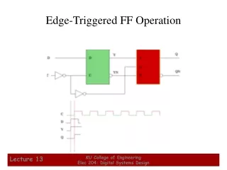
Edge-Triggered FF Operation
290 likes | 311 Vues
Edge-Triggered FF Operation. Edge-Triggered FF Operation. Edge-Triggered FF Operation. Edge-Triggered FF Operation. Flip-Flop Timing Parameters. t. t. $. wH. wH,min. t. t. $. C. wL. wL,min. t. t. s. h. /. R. S. t s - setup time t h - hold time t w - clock pulse width

Edge-Triggered FF Operation
E N D
Presentation Transcript
Edge-Triggered FF Operation KU College of Engineering Elec 204: Digital Systems Design
Edge-Triggered FF Operation KU College of Engineering Elec 204: Digital Systems Design
Edge-Triggered FF Operation KU College of Engineering Elec 204: Digital Systems Design
Edge-Triggered FF Operation KU College of Engineering Elec 204: Digital Systems Design
Flip-Flop Timing Parameters t t $ wH wH,min t t $ C wL wL,min t t s h / R S • ts - setup time • th - hold time • tw - clockpulse width • tpx - propagation delay • tPHL - High-to-Low • tPLH - Low-to-High • tpd - max (tPHL, tPLH) t p-,min t p-,max Q (a) Pulse-triggered (positive pulse) t t $ wH,min wH t t $ C wL wL,min t t s h D t p-,min t p-,max Q (b) Edge-triggered (negative edge) KU College of Engineering Elec 204: Digital Systems Design
Flip-Flop Timing Parameters (continued) • ts - setup time • Master-slave - Equal to the width of the triggering pulse • Edge-triggered - Equal to a time interval that is generally much less than the width of the the triggering pulse • th – minimum hold time for the inputs - Often equal to zero • tpx - propagation delay • Same parameters as for gates except • Measured from clock edge that triggers the output change to the output change KU College of Engineering Elec 204: Digital Systems Design
Inputs Combina-tional Logic Outputs Storage Elements Next State State CLK Sequential Circuit Analysis • General Model • Current Stateat time (t) is stored in an array oflip-flops. • Next State at time (t+1) is a Boolean function of State and Inputs. • Outputs at time (t) are a Boolean function of State (t) and (sometimes) Inputs (t). KU College of Engineering Elec 204: Digital Systems Design
x A Q D A Q C B Q D CP Q C y Example 1 (from Fig. 6-17) • Input: x(t) • Output:y(t) • State: (A(t), B(t)) • What is the Output Function? • What is the Next State Function? KU College of Engineering Elec 204: Digital Systems Design
Example 1 (from Fig. 6-17) (continued) • Boolean equations for the functions: • A(t+1) = A(t)x(t) + B(t)x(t) • B(t+1) = A(t)x(t) • y(t) = x(t)(B(t) + A(t)) x A Q D A Q C Next State B Q D CP Q' C y Output KU College of Engineering Elec 204: Digital Systems Design
1 0 1 0 0 0 1 0 Example 1(from Fig. 6-17) (continued) • Where in time are inputs, outputs and states defined? KU College of Engineering Elec 204: Digital Systems Design
State Table Characteristics • State table – a multiple variable table with the following four sections: • Present State – the values of the state variables for each allowed state. • Input – the input combinations allowed. • Next-state – the value of the state at time (t+1) based on the present state and the input. • Output – the value of the output as a function of the present state and (sometimes) the input. • From the viewpoint of a truth table: • the inputs are Input, Present State • and the outputs are Output, Next State KU College of Engineering Elec 204: Digital Systems Design
Present State Input Next State Output A(t) B(t) x(t) A(t+1) B(t+1) y(t) 0 0 0 0 0 0 0 0 1 0 1 0 0 1 0 0 0 1 0 1 1 1 1 0 1 0 0 0 0 1 1 0 1 1 0 0 1 1 0 0 0 1 1 1 1 1 0 0 Example 1: State Table (from Fig. 6-17) • The state table can be filled in using the next state and output equations: A(t+1) = A(t)x(t) + B(t)x(t) B(t+1) =A (t)x(t) y(t) =x (t)(B(t) + A(t)) KU College of Engineering Elec 204: Digital Systems Design
Present Next State Output State x(t)=0 x(t)=1 x(t)=0 x(t)=1 A(t) B(t) A(t+1)B(t+1) A(t+1)B(t+1) y(t) y(t) 0 0 0 0 0 1 0 0 0 1 0 0 1 1 1 0 1 0 0 0 1 0 1 0 1 1 0 0 1 0 1 0 Example 1: Alternate State Table • 2-dimensional table that matches well to a K-map. Present state rows and input columns in Gray code order. • A(t+1) = A(t)x(t) + B(t)x(t) • B(t+1) =A (t)x(t) • y(t) =x (t)(B(t) + A(t)) KU College of Engineering Elec 204: Digital Systems Design
State Diagrams • The sequential circuit function can be represented in graphical form as a state diagram with the following components: • A circle with the state name in it for each state • A directed arc from the Present State to the Next State for each state transition • A label on each directed arc with the Input values which causes the state transition, and • A label: • On each circle with the output value produced, or • On each directed arc with the output value produced. KU College of Engineering Elec 204: Digital Systems Design
State Diagrams • Label form: • On circle with output included: • state/output • Moore type output depends only on state • On directed arc with the output included: • input/output • Mealy type output depends on state and input KU College of Engineering Elec 204: Digital Systems Design
x=0/y=0 x=0/y=1 x=1/y=0 A B 1 0 0 0 x=0/y=1 x=1/y=0 x=1/y=0 x=0/y=1 1 1 0 1 x=1/y=0 Example 1: State Diagram • Which type? • Diagram getsconfusing forlarge circuits • For small circuits,usually easier tounderstand thanthe state table KU College of Engineering Elec 204: Digital Systems Design
Moore and Mealy Models • Sequential Circuits or Sequential Machines are also called Finite State Machines (FSMs). Two formal models exist: • In contemporary design, models are sometimes mixed Moore and Mealy • Moore Model • Named after E.F. Moore. • Outputs are a function ONLY of states • Usually specified on the states. • Mealy Model • Named after G. Mealy • Outputs are a function of inputs AND states • Usually specified on the state transition arcs. KU College of Engineering Elec 204: Digital Systems Design
x=1/y=0 x=0/y=0 1 0 x=0/y=0 x=1/y=1 x=0 0/0 x=0 x=1 x=1 x=0 2/1 1/0 x=1 Moore and Mealy Example Diagrams • Mealy Model State Diagrammaps inputs and state to outputs • Moore Model State Diagram maps states to outputs KU College of Engineering Elec 204: Digital Systems Design
Present Next State Output State x=0 x=1 x=0 x=1 0 0 1 0 0 1 0 1 0 1 Present Next State Output State x=0 x=1 0 0 1 0 1 0 2 0 2 0 2 1 Moore and Mealy Example Tables • Mealy Model state table maps inputs and state to outputs • Moore Model state table maps state to outputs KU College of Engineering Elec 204: Digital Systems Design
A D Z Q Q C R B D Q Q C R C D Q Clock Q C R Reset Example 2: Sequential Circuit Analysis • Logic Diagram: KU College of Engineering Elec 204: Digital Systems Design
Example 2: Flip-Flop Input Equations • Variables • Inputs: None • Outputs: Z • State Variables: A, B, C • Initialization: Reset to (0,0,0) • Equations • A(t+1) = Z = • B(t+1) = • C(t+1) = KU College of Engineering Elec 204: Digital Systems Design
Example 2: State Table X+ = X(t+1) KU College of Engineering Elec 204: Digital Systems Design
ABC Reset 000 111 100 001 101 011 010 110 Example 2: State Diagram • Which states are used? • What is the function ofthe circuit? KU College of Engineering Elec 204: Digital Systems Design
D Q D Q C C Q' Q' D Q D Q C C Q' Q' D Q D Q C C Q' Q' D Q D Q C C Q' Q' D Q D Q C C Q' Q' CLOCK CLOCK Circuit and System Level Timing • Consider a systemcomprised of ranksof flip-flopsconnected by logic: • If the clock period istoo short, somedata changes will notpropagate through thecircuit to flip-flop inputs before the setuptime interval begins KU College of Engineering Elec 204: Digital Systems Design
t p C t t t t pd,FF pd,COMB s slack (a) Edge-triggered (positive edge) t p C t t t t pd,FF pd,COMB slack s (b) Pulse-triggered (negative pulse) Circuit and System Level Timing (continued) • Timing components along a path from flip-flop to flip-flop KU College of Engineering Elec 204: Digital Systems Design
Circuit and System Level Timing (continued) • New Timing Components • tp - clock period - The interval between occurrences of a specific clock edge in a periodic clock • tpd,COMB - total delay of combinational logic along the path from flip-flop output to flip-flop input • tslack - extra time in the clock period in addition to the sum of the delays and setup time on a path • Can be either positive or negative • Must be greater than or equal to zero on all paths for correct operation KU College of Engineering Elec 204: Digital Systems Design
Circuit and System Level Timing (continued) • Timing Equations tp = tslack + (tpd,FF + tpd,COMB + ts) • For tslack greater than or equal to zero,tp≥ max (tpd,FF + tpd,COMB + ts)for all paths from flip-flop output to flip-flop input • Can be calculated more precisely by using tPHL and tPLH values instead of tpd values, but requires consideration of inversions on paths KU College of Engineering Elec 204: Digital Systems Design
Calculation of Allowable tpd,COMB • Compare the allowable combinational delay for a specific circuit:a) Using edge-triggered flip-flops b) Using master-slave flip-flops • Parameters • tpd,FF(max) = 1.0 ns • ts(max) = 0.3 ns for edge-triggered flip-flops • ts = twH = 1.0 ns for master-slave flip-flops • Clock frequency = 250 MHz KU College of Engineering Elec 204: Digital Systems Design
Calculation of Allowable tpd,COMB (continued) • Calculations: tp = 1/clock frequency = 4.0 ns • Edge-triggered: 4.0 ≥ 1.0 + tpd,COMB + 0.3, tpd,COMB ≤ 2.7 ns • Master-slave: 4.0 ≥ 1.0 + tpd,COMB + 1.0, tpd,COMB ≤ 2.0 ns • Comparison: Suppose that for a gate, average tpd = 0.3 ns • Edge-triggered: Approximately 9 gates allowed on a path • Master-slave: Approximately 6 to 7 gates allowed on a path KU College of Engineering Elec 204: Digital Systems Design