Download
1 / 37
370 likes | 520 Vues
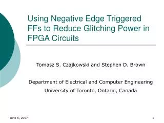
Using Negative Edge Triggered FFs to Reduce Glitching Power in FPGA Circuits. Tomasz S. Czajkowski and Stephen D. Brown Department of Electrical and Computer Engineering University of Toronto, Ontario, Canada. Motivation. Glitches:

E N D
Using Negative Edge Triggered FFs to Reduce Glitching Power in FPGA Circuits Tomasz S. Czajkowski and Stephen D. Brown Department of Electrical and Computer Engineering University of Toronto, Ontario, Canada
Motivation • Glitches: • Undesirable logic transitions that occur due to delay imbalance in the logic circuit • Waste power and do not provide any useful functionality • Can increase the average toggle rate of a net by as much as a factor of 2 • Not well defined until post placement and routing • Glitches can be filtered out by strategically inserting negative edge triggered FFs
Due to unequal arrival time of signals at the inputs of LUTs Glitches can be propagated through LUTs Generated 4LUT Propagated 4LUT Glitches in FPGAs
Insert a negative edge triggered FF after a LUT that produces or propagates glitches Generated Reducing Glitches 4LUT 4LUT No glitches clock
Alternatives • Gated D-latch • Implement a gated D-latch in a LUT • Input signal is transparent during the latter halfof the clock period • Gated LUT • Gate the output of a LUT with the clock input using an AND or an OR gate • Similar effect as gated D-latch • Can generate glitches too • When implemented • Gated D-latch consumes 50% more power thana FF and double that of a gated LUT • Neither alternative is very effective
Background on Dynamic Power • Average Net Dynamic Power Dissipation • Pavg is average power • V is supply voltage • fclock is the clock frequency • si is the average per cycle toggle rate of a net • Ci is the capacitance of a net
Power Model • Goal • To be able to compute the change in dynamic power dissipation in the logic elements affected by a negative edge triggered FF insertion • Power dissipated by a LUT and a FF • Toggle Rate of logic signals (si) • Net capacitance (Ci)
LUT Power • The LUT itself dissipates an non-trivial amount of power when its inputs toggle • We look at how the power dissipated by a LUT relates to the frequency of its output transitions
FF Power • How much power would it cost to insert a FF into a circuit? • What about the power cost of alternatives to a FFs? • Gated LUT • Gated D-latch
Toggle Rate of Logic Signals • Topic is covered considerably in literature • Toggle rate model based on the concept of Transition Density [Najm’94] and the work of Anderson and Najm [AN’03] • The latter work decomposes transition density into transitions generated by a LUT and that propagated through a LUT. • Modified to include delay information in order to account for glitches
Examples of Wires Clock A B C D
y z x Propagating Glitches Through a LUT • Increase D(z) to account for glitches that occur on wire y (D(y)-Pt(y)). Do so only when x remains at constant 1 for the duration of the clock cycle.
Net Capacitance • We need to be able to estimate net capacitance to figure out the difference in dynamic power dissipation due to a change in the transition density of a net • Relate net capacitance (unavailable directly) to net delay (available through timing report) • Distinguish between nets of different fanout
Higher Fanout Net Capacitance • In our benchmark set fewer than 5% of the nets had fanout greater than 4 • Clock net is excluded from calculation • Approximate capacitance of net with fanout n>4 as: • Not exact, but supports the fact that glitches on nets with high fanout are bad • Average estimate error of +22%
Negative Edge Triggered FF Insertion Algorithm • Scan all nets in a logic circuit to determine if negative edge FF insertion can be applied • Analyze the resulting set of nets to determine the benefit of applying the optimization to each net (determined by the cost function) • Apply the optimization to a net on which the most power could be saved • Repeat until no beneficial choices are found
Cost Function • Compute change in power (∆P) • + cost of adding a FF • - power saved on the modified net • - power saved on nets and LUTs in the transitive fanout of the added FF • Compute the change in the minimum clock period (∆T) • Specify ∆T allowed (∆Ta) • where u(x) is the step function • Accept change when ∆C < 0
Some logic network Example LUT FF LUT LUT LUT FF LUT LUT FF
Some logic network Example: Inserted FF LUT FF LUT LUT Neg FF LUT FF LUT LUT FF
Some logic network Example: Compute change in the # of glitches LUT FF LUT LUT Neg FF LUT FF LUT LUT FF
Some logic network Example: Compute change in the # of glitches LUT FF LUT LUT Neg FF LUT FF LUT LUT FF
Some logic network Example: Compute change in LUT power dissipation LUT FF LUT LUT Neg FF LUT FF LUT LUT FF
Experimental Results • 8 benchmark circuits taken from QUIP package • Synthesize, place, route and analyze timing of a circuit using Quartus II 5.1 • Apply algorithm to reduce glitches in a circuit • Aim to decrease the minimum clock period by no more than 5% • Perform timing analysis once the circuit has been modified • Use ModelSIM-Altera 6.0c for simulation • Simulate a circuit both pre- and post- modification using the same clock frequency • Use PowerPlay Power analyzer to estimate the average dynamic power dissipation of each circuit
Observations (1) • oc_des_perf_opt • Large number of XOR gates present • Removing glitches from one node removes a lot of glitches on the nodes in its transitive fanout (up to the next FF) • mux64_16bit • The cost function determined that no net was a good candidate for optimization • Very few glitches were present in the circuit and the power they dissipate was not large enough to warrant the insertion of FFs
Observations (2) • cf_fir_24_8_8 • Overestimated toggle rate caused the algorithm to apply negative edge triggered FF insertion too excessively • Need to include spatial correlation in the toggle rate model • aes128_fast • Toggle rate is 50% higher than in oc_des_perf_opt • Most nets use local LAB connections, causing little power dissipation • Insertion of 173 FFs only achieved 1% power reduction • Saved 35.14 mW in routing alone, because toggle rate on all affected wires was reduced by 50-70% • Added 24.6 mW due to FF insertion • Added 1.86 mW to the power dissipated by the clock network, because new LABs were connected to the clock network • Net win of 8.68 mW
Conclusion • Negative edge triggered FF insertion can work well to reduce glitches in a circuit • Computing glitches propagated to the transitive fanout of a net is important, especially when XOR gates are present • When inserting a lot of negative edge triggered FFs, be mindful where they go. Do target LABs have a clock signal already routed to them? • Unlike retiming, our approach only needs to ensure that exactly one negative edge triggered FF is on any given combinational path • Retiming may require the translation of more than a single FF to be valid
Future Work • Better toggle rate prediction algorithm that includes spatial correlation • Having FFs that can be negative edge triggered without using an additional LAB clock line would make the cost of this optimization lower • Silicon area cost vs. frequency of use trade-off
Acknowledgement • We’d like to express our gratitude to Altera for funding this research • We’d like to thank Altera Toronto in particular for dedicating some of their time to answer our questions and provide insight throughout the course of this work