
Purpose of This Chapter • To implement a stored program computer which can execute a set of instructions .
5 Computer Organization. Purpose of This Chapter • To implement a stored program computer which can execute a set of instructions . (A stored program computer behaves as different machines by loading different programs, i.e., sequences of instructions.).

Purpose of This Chapter • To implement a stored program computer which can execute a set of instructions .
E N D
Presentation Transcript
5 Computer Organization • Purpose of This Chapter • • To implement a stored program computer which can execute a set of instructions. • (A stored program computer behaves as different machines by loading different programs, i.e., sequences of instructions.) Slides for Chapter 5 prepared by Dr. Saeid Belkasim, Dept. of Computer Science, GSU
• Computer hardware = registers + ALU + datapath (bus) + control unit. • The computer goes through instruction cycles: i) Fetch an instruction from memory; ii) Decode the instruction to a sequence of control signals; iii) Execute the decoded sequence of microoperations. • Control unit: Instruction ® a time sequence of control signals to trigger microoperations. • Input-output is implemented using an interrupt cycle.
5-1. Instruction Codes • Stored Program Organization : Fig. 5-1 • The simplest way to organize a computer • One processor register : AC(Accumulator) • The operation is performed with the memory operand and the content of AC • Instruction code format with two parts : Op. Code + Address • Op. Code : specify 16 possible operations(4 bit) • Address : specify the address of an operand(12 bit) • If an operation in an instruction code does not need an operand from memory, the rest of the bits in the instruction(address field) can be used for other purpose • Memory : 12 bit = 4096 word(Instruction and Data are stored) • Store each instruction code(program) and operand (data) in 16-bit memory word Example Clear AC, Increment AC, Complement AC, ...
I=0 : Direct, I=1 : Indirect • Addressing Mode • Immediate operand address : • the second part of instruction code(address field) specifies operand • Direct operand address : Fig. 5-2(b) • the second part of instruction code specifies the address of operand • Indirect operand address : Fig. 5-2(c) • the bits in the second part of the instruction designate an address of a memory word in which the address of the operand is found (Pointer) • One bit of the instruction code is used to distinguish between a direct and an indirect address : Fig. 5-2(a) • Effective address: Address where an operand is physically located
AR IR DR Direct Addressing Occurs When the Operand Part Contains the Address of Needed Data. 1 1 0 1 0 1 0 1 1 0 0 1 1. Address part of IR is placed on the bus and loaded back into the AR 0 1 0 1 1 0 0 1 Memory 2. Address is selected in memory and its Data placed on the bus to be loaded into the Data Register to be used for requested instructions 0 0 0 0 0 0 0 0 1 1 1 1
AR IR DR Indirect Addressing Occurs When the Operand Contains the Address of the Address of Needed Data. 1 1 0 1 0 1 0 1 1 0 0 1 1. Address part of IR is placed on the bus and loaded back into the AR 0 1 0 1 1 0 0 1 1 0 1 1 1 0 1 1 2. Address is selected in memory and placed on the bus to be loaded Back into the AR Memory 3. New Address is selected in memory and placed on the bus to be loaded into the DR to use later 0 0 0 0 0 0 0 0 0 1 0 1
5-2 Computer Registers • Data Register(DR) : hold the operand(Data) read from memory • Accumulator Register(AC) : general purpose processing register • Instruction Register(IR) : hold the instruction read from memory • Temporary Register(TR) : hold a temporary data during processing • Address Register(AR) : hold a memory address, 12 bit width • Program Counter(PC) : • hold the address of the next instruction to be read from memory after the current instruction is executed • Instruction words are read and executed in sequence unless a branch instruction is encountered • A branch instruction calls for a transfer to a nonconsecutive instruction in the program • The address part of a branch instruction is transferred to PC to become the address of the next instruction • To read instruction, memory read cycle is initiated, and PC is incremented by one(next instruction fetch)
Input Register(INPR) : receive an 8-bit character from an input device • Output Register(OUTR) : hold an 8-bit character for an output device The following registers are used in Mano’s example computer. Register Number Register Register symbol of bits name Function----------------------- DR 16 Data register Holds memory operands AR 12 Address register Holds address for memory AC 16 Accumulator Processor register IR 16 Instruction register Holds instruction code PC 12 Program counter Holds address of instruction TR 16 Temporary register Holds temporary data INPR 8 Input register Holds input character OUTR 8 Output register Holds output character
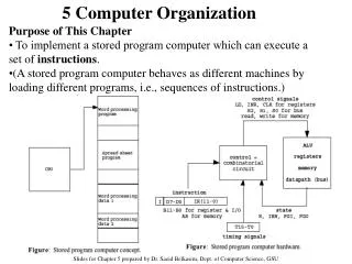
Mano’s Computer Figure 5-4 s0 s1 s2 Bus Memory Unit 4096x16 7 Address WRITE READ 1 AR CLR LD INR 2 PC CLR LD INR 3 DR LD CLR INR E Adder & Logic 4 AC LD CLR INR INPR 5 IR LD TR 6 INR CLR LD OUTR Clock LD 16-bit common bus Computer System Architecture, Mano, Copyright (C) 1993 Prentice-Hall, Inc.
Common Bus System • The basic computer has eight registers, a memory unit, and a control unit. • Paths must be provided to transfer information from one register to another and between memory and registers • A more efficient scheme for transferring information in a system with many registers is to use a common bus. • The connection of the registers and memory of the basic computer to a common bus system : Fig. 5-4 • The outputs of seven registers and memory are connected to the common bus • The specific output is selected by mux(S0, S1, S2) : • Memory(7), AR(1), PC(2), DR(3), AC(4), IR(5), TR(6) • When LD(Load Input) is enable, the particular register receives the data from the bus • Control Input : LD, INC, CLR, Write, Read
COMMON BUS SYSTEM • • Control variables: Various control variables are used to select: • the paths of information; & • the operation of the registers. • Selection variables: Used to specify a register whose output is connected to the common bus at any given time. • To select one register out of 8, we need 3 select variables. • For example, if S2S1S0 = 011, the output of DR is directed to the common bus. • > Load input (LD): Enables the input of a register connected to the common bus. When LD = 1 for a register, the data on the common bus is read into the register during the next clock pulse transition. • > Increment input (INR): Increments the content of a register. • > Clear input (CLR): Clear the content of a register to zero. • • When the contents of AR or PC (12 bits) are applied to the 16-bit common bus, the four most significant bits are set to zero. When AR or PC receives information from the bus, only the 12 least significant bits are transferred to the register. Both INPR and OUTR use only the 8 least significant bits of the bus.
Mano’s Computer: Memory Words 0 15 12 11 • 4-bit opcode Bits 15-12 • How many possible instructions? • 24=16 • This leaves 12 bits for the address • How many words of memory? • 212 = 22•210 = 4K = 4096 16-bit words
Mano's Computer: Instructions 0 15 12 11 • 24 = 16 possible instructions • Op-code 0111 reserved for register-reference instructions • How many possible register-reference instructions? • 212 = 22•210 = 4K = 4096 possible r-r instructions(only 12 are used)
Mano's Computer: Instructions 0 15 12 11 • 24 = 16 possible instructions • Op-code 1111 reserved for input/output instructions • 24 = 16 possible instructions - 0111 (r-r) - 1111 (i/o) = 14 instructions left • These are coded as 7 instructions with direct and indirect addressing
15 14 12 11 0 15 14 12 11 0 15 14 12 11 0 I Opcode Address 0 1 1 1 Register Operation 1 1 1 1 I/O Operation 5-3. Computer Instruction • 3 Instruction Code Formats : Fig. 5-5 • Memory-reference instruction • Opcode = 000 110 • I=0 : 0xxx ~ 6xxx, I=1: 8xxx ~Exxx • Register-reference instruction • 7xxx (7800 ~ 7001) : CLA, CMA, • Input-Output instruction • Fxxx(F800 ~ F040) : INP, OUT, ION, SKI, I=0 : Direct, I=1 : Indirect Reading this table: the presented code is for any instruction that has 16 bits. The xxx represents don’t care ( any data for the first 12 bits). Example 7002 for is a hexadecimal code equivalent to 0111 0000 0000 0010 Which means B1 (Bit 1) is set to 1 and the rest of the first 12 bits are set to zeros.
• Instructions are normally stored in consecutive memory locations and are executed sequentially one at a time. • The program counter (PC) holds the address of the next instruction to be read from memory after the current instruction is executed. • The PC has 12 bits like the AR. • The instruction read from memory is placed in the instruction register (IR) which has 16 bits corresponding to our instruction code length. • • Most processing takes place in the accumulator (AC); • the temporary register (TR) is used for holding temporary data during the processing. • • The input (INPR) and output (OUTR) registers hold a character at a time which is read from an input device or to be printed to an output device, respectively. Using the ASCII code, one character is represented with 8 bits (1 byte).
5-4. Timing and Control • Microprogrammed Control : Chap. 7 • The control information is stored in a control memory, and the control memory is programmed to initiate the required sequence of microoperations • + Any required change can be done by updating the microprogram in control memory, - Slow operation • Control Unit : Fig. 5-6 • Control Unit = Control Logic Gate + 3 X 8 Decoder + Instruction Register + Timing Signal • Timing Signal = 4 X 16 Decoder + 4-bit Sequence Counter • Example) Control timing : Fig. 5-7 • Sequence Counter is cleared when D3T4 =1 : • Memory R/W cycle time > Clock cycle time
CONTROL UNIT HARDWARE • Inputs to the control unit come from IR where an instruction read from the memory unit is stored. • A hardwired control is implemented in the example computer using: > A 3 ´ 8 decoder to decode opcode bits 12-14 into signals D0, ..., D7; > A 4-bit binary sequence counter (SC) to count from 0 to 15 to achieve time sequencing; > A 4 ´ 16 decoder to decode the output of the counter into 16 timing signals, T0, ..., T15 > A flip-flop (I) to store the addressing mode bit in IR; > A digital circuit with inputs—D0, ..., D7, T0, ..., T15, I, and address bits (11-0) in IR—to generate control outputs supplied to control inputs and select signals of the registers and the bus. • Clocking principle: The binary counter goes through a cycle, 0000 ® 0001 ® 0010 ® ... ® 1111 ® 0000. Accordingly only one of T0, ..., T15 is 1 at each clock cycle, T0 ® T1 ® T2 ® ... ® T15 ® T0; all the other timing signals are 0. • By setting the clear input (CLR) of SC at a clock cycle, say T3, we can achieve a 4-cycle clock: T0 ® T1 ® T2 ® T3 ® T0.
5.5 Instruction Cycle • A computer goes through the following instruction cycle repeatedly: do 1. Fetch an instruction from memory 2. Decode the instruction 3. Read the effective address from memory if the instruction has an indirect address 4. Execute the instruction until a HALT instruction is encountered • The fetch & decode phases of the instruction cycle consists of the following microoperations synchronized with the timing signals (clocking principle). Timing signal microoperations T0: AR ¬ PC T1: IR ¬ M[AR], PC ¬ PC + 1 T2: D0, ..., D7 ¬ Decode IR(12-14), AR ¬ IR(0-11), I ¬ IR(15)
T0: Since only AR is connected to the address inputs of memory, the address of instruction is transferred from PC to AR. 1. Place the content of PC onto the bus by making the bus selection inputs S2S1S0 = 010. 2. Transfer the content of the bus to AR by enabling the LD input to AR ( AR ¬ PC). T1: The instruction read from memory is then placed in the instruction register IR. At the same time, PC is incremented to prepare for the address of the next instruction. 1. Enable the read input of the memory. 2. Place the content of memory onto the bus by making the bus selection inputs S2S1S0 = 111. (Note that the address lines are always connected to AR, and we have already placed the next instruction address in AR.) 3. Transfer the content of the bus to IR by enabling the LD input to IR (IR ¬ M[AR]). 4. Increment PC by enabling the INR input of PC ( PC ¬ PC + 1 ). T2: The operation code in IR is decoded; the indirect bit is transferred to I; the address part of the instruction is transferred to AR. (See the common bus skeleton diagram.)
Similar circuits are used to realize the microoperations at T2. • At T3, microoperations which take place depend on the type of instruction. The four different paths are symbolized as follows, where the control functions must be connected to the proper inputs to activate the desired microoperations. Control function Microoperation D7’IT3: AR ¬ M[AR], indirect memory transfer D7’I’T3: Nothing, direct memory transfer D7I’T3: Execute a register-reference instruction D7IT3: Execute an I/O instruction When D7’T3 = 1 (At T3 & IR(12-14) ¹ 111), the execution of memory-reference instructions takes place with the next timing variable T4.
Figure: Control circuit for instruction fetch. This is a part of the control circuit and demonstrates the kind of wiring needed.
REGISTER-REFERENCE INSTRUCTIONS • The 12 register-reference instructions are recognized by I = 0 and D7 = 1 (IR(12-14) = 111). Each operation is designated by the presence of 1 in one of the bits in IR(0-11). Therefore D7I’T3 º r = 1 is common to all register-transfer instructions.
5.6 Memory Reference Instructions • Opcode (000 - 110) or the decoded output Di (i = 0, ..., 6) are used to select one memory-reference operation out of 7.
0 BSA 135 next instruction 21(return address) Subroutine 1 BUN 135 PC = 10 PC = 21 135 PC = 136 5-6. Memory Reference Instruction Fig. 5-10 Example of BSA • STA : memory write • BUN : branch unconditionally • BSA : branch and save return address • Return Address : save return address ( 135 21 ) • Subroutine Call : Fig. 5-10 • ISZ : increment and skip if zero • Control Flowchart : Fig. 5-11 • Flowchart for the 7 memory reference instruction • The longest instruction : ISZ(T6) • 3 bit Sequence Counter
Branch and Save Address (BSA) Subroutine implementation using BSA.
5-7. Input-Output and Interrupt • 5-7 Input-Output and Interrupt • Input-Output Configuration : Fig. 5-12 • Input Register(INPR), Output Register(OUTR) • These two registers communicate with a communication interface serially and with the AC in parallel • Each quantity of information has eight bits of an alphanumeric code • Input Flag(FGI), Output Flag(FGO) • FGI : set when INPR is ready, clear when INPR is empty • FGO : set when operation is completed, clear when output device is in the process of printing • Input-Output Instruction : Tab. 5-5 • p = D7IT3 • IR(i) = Bi IR(6 -11) • B6 - B11 : 6 I/O Instruction • Program Interrupt • I/O Transfer Modes • 1) Programmed I/O, 2) Interrupt-initiated I/O, 3) DMA, 4) IOP • 2) Interrupt-initiated I/O (FGI FGO 1 Int. ) • Maskable Interrupt ( ION IOF Int. mask ) 1 : Ready 0 : Not ready Address
Interrupt Cycle : Fig. 5-13 During the execute phase, IEN is checked by the control IEN = 0 : the programmer does not want to use the interrupt, so control continues with the next instruction cycle IEN = 1 : the control circuit checks the flag bit, If either flag set to 1, R (R is the interrupt flip flop ) is set to 1 At the end of the execute phase, control checks the value of R R = 0 :instruction cycle R = 1 : Interrupt cycle Demonstration of the interrupt cycle : Fig. 5-14 The memory location at address 0 as the place for storing the return address Interrupt Branch to memory location 1 Interrupt cycle IEN=0 (ISRInterrupt ION) The condition for R = 1 Modified Fetch Phase Modified Fetch and Decode Phase 256(return address) 0 BUN 1120 Main Program Interrupt Service Routine 1 BUN 0 0 PC = 1 255 256 1120 Interrupt Here Save Return Address(PC) at 0 Jump to 1(PC=1)
5-8. Complete Computer Description • 5-8 Complete Computer Description • The final flowchart of the instruction cycle : Fig. 5-15 • The control function and microoperation : Table. 5-6 • 5-9 Design of Basic Computer • The basic computer consists of the following hardware components • 1. A memory unit with 4096 words of 16bits • 2. Nine registers : AR, PC, DR, AC, IR, TR, OUTR, INPR, and SC(Fig. 2-11) • 3. Seven F/Fs : I, S, E, R, IEN, FGI, and FGO • 4. Two decoders in control unit : 3 x 8 operation decoder, 4 x 16 timing decoder(Fig. 5-6) • 5. A 16-bit common bus(Fig. 5-4) • 6. Control Logic Gates : Fig. 5-6 • 7. Adder and Logic circuit connected to the AC input • Control Logic Gates • 1. Signals to control the inputs of the nine registers • 2. Signals to control the read and write inputs of memory • 3. Signals to set, clear, or complement the F/Fs • 4. Signals for S2 S1 S0 to select a register for the bus • 5. Signals to control the AC adder and logic circuit
Since memory is 4K in size, it requires 12 address bits. Each word of memory contains 16 bits of data. Similarly, the program counter (PC) is also 12 bits wide. Each data word is 16 bits wide. The Data Register (DR) must also be 16 bits wide, since it receives data from and sends data to memory. The accumulator (AC) acts on 16 bits of data. The Instruction Register (IR) receives instruction codes from memory which are 16 bits wide. Basic Computer specification u 4K x 16 RAM u 12-bit AR, PC u 16-bit DR, AC, IR, TR u 8-bit INPR, OUTR u 3-bit SC u 1-bit E, I, IEN, FGI, FGO TR is a temporary register. Only the CPU can cause it to be accessed. The programmer cannot directly manipulate the contents of TR. Most CPU’s have one or more temporary registers which it uses to perform instructions. The input and output registers (INPR and OUTR) are 8 bits wide each. For this CPU, I/O instructions only transfer 8 bits of data at a time. The 3-bit sequence counter (SC) is used to generate the correct timing (T) states. Other 1-bit registers are the carry out (E), the indirect register (I), the interrupt enable (IEN) and the input and output flags (FGI and FGO).
The control unit must make sure that at most one register (or memory unit) places data onto the bus at one time. • The memory unit is external to the CPU. It always receives its address from the address register (AR) and makes its data available to the CPU bus. It receives data from the CPU bus as well. • Read and write signals are supplied by the control unit. • The address registers, program counter (PC) and data register (DR) each load data onto and receive data from the system bus. Each has a load, increment and clear signal derived from the control unit. These signals are synchronous; each register combines these signals with the system clock to activate the proper function. • Since AR and PC are only 12-bits each, they use the low order 12 bits of the bus.
The accumulator makes its data available on the bus but does not receive data from the bus. • it receives data from ALU (Adder and Logic) only. • To load data into AC, place it onto the bus via DR and pass it directly through the ALU. • Note that E, the 1-bit carry flag, also receives its data from the ALU. • The input register, INPR, receives data from an external input port and makes it available only to AC. • The output register makes its data available to the output port using specific hardware. • The instruction register, IR, can only be loaded; it cannot be incremented nor cleared. Its output is used to generate Di’s and Ti’s control signals. • TR is a temporary register. The CPU uses this register to store intermediate results of operations. It is not accessible by the external programs. It is loaded, incremented and cleared like the other registers.
Register reference instructions are those which access data and manipulate the contents of registers. • They do not access memory. • These instructions are executed in one clock cycle. • Each register reference instruction is performed in a single clock cycle. • Each instruction manipulates the contents of a register within the CPU, so the relatively time consuming accesses to memory are avoided. • There are 12 register reference instructions overall, each of which is encoded by one of the 12 low order bits of the instruction code.
This class of instructions accesses I/O devices. • The instructions in this class also enable and disable interrupts. Since this computer only allows for a single input device and a single output device, no address information is needed. • The input/output instructions are performed in a single clock cycle. • Note that there are no instructions to set FGI or FGO to 1. • These flags are set by external hardware when input data is ready or output data is requested. When the CPU performs the proper input or output instruction (INP or OUT), it resets the flag to allow for future I/O data transfers.
Control signals u T0, T1, ... T6 : Timing signals u D0, D1, ... D7 : Decoded instruction u I: Indirect bit u R: Interrupt cycle bit • The T signals occur in sequence and are never skipped over. The only two options during a T-state are to proceed to the next T-state or to return to T state 0. • The D signals decode the instruction and are used to select the correct execute routine. • I is used to select the indirect routine and also to select the correct execute routine for non-memory reference instructions. • R is used for interrupt processing and will be explained later.
Control signals This circuit generates the T signals. The sequence counter, SC, is incremented once per clock cycle. Its outputs are fed into a 3-8 decoder which generates the T signals. Whenever a micro-operation sets SC to zero, it resets the counter, causing T0 to be activated during the next clock cycle.
Control signals The D signals are generated in a similar way as the T signals. For the D signals the source is IR(14-12) instead of SC. Also note that IR won’t change during the instruction execution.
Fetch and indirect cycles Example: Fetch from 100: AND I 500; M[500] = 234 T0: AR ¬ 100 T1: IR ¬ 8500, PC ¬ 101 T2: AR ¬ 500, I ¬ 1, D0 ¬ 1 D7’IT3: AR ¬ M[500](11-0) = 234 • In this example, the instruction AND I 500 is fetched from memory location 100. • During T0, the address (100) is loaded into AR. • During T1, the instruction code is loaded into IR and PC is incremented. • In T2, the address portion of this instruction, 500, is loaded into AR. The indirect register gets 1, the value of the indirect bit of the instruction. Since bits 14-12 are 000, D0 is activated by the decoder. These tell us that we have an indirect AND instruction. • In T3, D7 is ‘0’ and I is ‘1’, the address portion of the instruction is not the address of the operand. It is the address of a memory location which contains address of actual operand. Look in memory to get the actual address, 234, which is loaded into AR.
AND execute cycle AND: D0T4: DR ¬ M[AR] D0T5: AC ¬ AC ^ DR, SC ¬ 0 Example: AND 500: AC = 31, M[500] = 25 D0T4: DR ¬ 25 D0T5: AC ¬ 31 ^ 25 = 21, SC ¬ 0 • In this and all examples, all data is given in hex. Here, the instruction cycle has fetched the AND instruction, determined that this execute routine must perform and load address 500 into the AR. • In T4, the data is read from memory and loaded into the DR, 25 in this case. Next, • in T5, it is logically ANDed with the current contents of the accumulator, 31 here, and the result is stored back into the accumulator. Setting SC to zero returns to the fetch routine to access the next instruction.
ADD execute cycle ADD: D1T4: DR ¬ M[AR] D1T5: AC ¬ AC + DR, SC ¬ 0 Example: ADD 500: AC = 31, M[500] = 25 D1T4: DR ¬ 25 D1T5: AC ¬ 31 + 25 = 56, SC ¬ 0 The ADD operation proceeds similarly to the AND operation. The only difference is that once the operand is loaded from memory it is arithmetically added to the current contents of the accumulator.
LDA execute cycle LDA: D2T4: DR ¬ M[AR] D2T5: AC ¬ DR, SC ¬ 0 Example: LDA 500: M[500] = 25 D2T4: DR ¬ 25 D2T5: AC ¬ 25, SC ¬ 0 As in the previous instructions, the CPU reads the data from memory into DR during T4. In the following cycle, this data is copied into the accumulator. Since the accumulator only receives data from the adder and logic section, the data from DR is passed into this unit and then passed through it unchanged.
STA execute cycle STA: D3T4: M[AR] ¬ AC, SC ¬ 0 Example: STA 500: AC = 31, M[500] = 25 D3T4: M[500] ¬ 31, SC ¬ 0 The STA instruction is much more straightforward than the LDA instruction. Since the address is already available from AR to the memory unit, we simply move data directly from the accumulator to the memory unit in a single clock cycle.
BUN execute cycle BUN: D4T4: PC ¬ AR, SC ¬ 0 Example: BUN 500 D4T4: PC ¬ 500, SC ¬ 0 The BUN instruction implements a jump by loading the new address directly from AR into the PC. Unlike many of the other memory reference instructions, BUN receives its data as part of the original instruction and does not require a secondary memory access.
BSA execute cycle BSA: D5T4: M[AR] ¬ PC, AR ¬ AR+1 D5T5: PC ¬ AR, SC ¬ 0 • The BSA instruction implements a subroutine call. • A BSA for address X stores the return address at location X. • Note that PC was incremented as part of the opcode fetch and thus contains the return address. AR contains X. • During T4, AR is incremented to X+1, since this is the start of the actual subroutine code. • T5 loads the value X+1 into the program counter and returns to the fetch routine. Note that this computer cannot implement recursion. If a subroutine called itself, it would overwrite the original return address and would be caught in the subroutine forever! We return from a subroutine by using a BUN I X instruction.
Subroutine call using BSA Example: 100: BSA 200 D5T4: M[AR] ¬ PC, AR ¬ AR+1 M[200] ¬ 101, AR ¬ 201 D5T5: PC ¬ AR, SC ¬ 0 PC ¬ 201, SC ¬ 0 • During T4, the return address, 101, is loaded into memory location 200 and AR is set to 201. This value is the location of the first instruction of the subroutine. • During T5 it is loaded into the program counter. • The computer will next fetch the instruction at this location.
Subroutine return using BUN I Example: 205: BUN I 200 M[200] = 101 D7I’T3: AR ¬ M[AR](11-0) AR ¬ M[200](11-0) = 101 D4T4: PC ¬ AR, SC ¬ 0 PC ¬ 101, SC ¬ 0 • In this example we perform a return from a previous subroutine. • After executing a few instructions which comprise the subroutine, we reach the BUN I 200 instruction. • During the indirect cycle, we go to location 200 to get the actual address we want, in this case 101. • During T4, we load this value into the program counter, affecting the jump.