Understanding Processor Performance: Key Elements and MIPS Instruction Implementation
This chapter delves into the crucial performance factors of processors, including instruction count, clock cycle time, and cycles per instruction (CPI). It explores how these metrics are influenced by processor implementation and presents two different datapath and control unit designs for core MIPS instructions. Key concepts like arithmetic operations, memory references, and branch instructions are discussed, alongside an overview of functional units and clocking methodologies. This foundation prepares you for constructing effective processors tailored to MIPS instruction execution.

Understanding Processor Performance: Key Elements and MIPS Instruction Implementation
E N D
Presentation Transcript
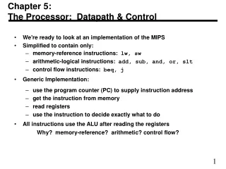
Chapter 5 - The Processor • Machine Performance factors • Instruction Count, Clock cycle time, Clock cycles per instruction (CPI) • Both clock cycle time and CPI are determined by processor implementation • We will construct datapath and a control unit for 2 different processor implementations for ‘core’ instructions • Memory ref: lw/sw • Arithmetic: add/sub/and/or/slt • Control: beq/j
Implementation Overview • Consider a core subset of MIPS instructions: • Integer arith-log instructions • Memory-reference instructions • Branch instructions • Good news is that much is similar across different instructions • For every instruction • Set the PC to a memory location to fetch an instruction • Read one or two registers using instructions fields to choose registers
Differing Instructions • After previous 2 steps, instructions diverge • All instructions do use the ALU next • Arith-log: for opcode execution • Mem-ref: for effective address calculation • Branches: for comparison • After using the ALU • Arith-log: write data from ALU to register • Mem-ref: access memory containing data to complete a store or retrieve a word being loaded • Branch: may need to exchange next instruction address based on comparison
High-level view • Two types of functional units: • elements that operate on data values (combinational) • elements that contain state (sequential)
Clocking methodology • Defines when signals can be read and when they can be written • Assume an edge-triggered clock • Clock cycles between high and low • Clock period: time for one full cycle
MIPS subset implementation • Develop 2 implementations • Single long clock cycle for each instruction (simple) • Multiple clock cycles per instructions (complex) • Input / Output • Nearly all elements have 32 bit wide inputs/outputs • Buses: signals > 1 bit (thick lines) • Control signals vs data signals • Notation: control in colour
Building Blocks • Instruction Memory: a place to store program instructions • Program Counter (PC): the address of an instruction • Adder: to increment the PC to the instruction location
The common bit • Instruction execution • Fetch instruction from memory • Increment PC to next instruction (PC += 4)
R-format • add, sub, slt, and, or • E.g add $1,$2,$3 ($1 = $2+$3) • Need fourth element: Register file • Contains register state of the machine • Register can be read or written by specifying number • 2 read ‘ports’ and 1 write ‘port’ • 32 registers => 5 bit register number • Fifth element: ALU • 3 bit operation signal
R-format execution • Only two elements required • Read 2 registers • Perform ALU operation on the contents of the registers • Write the result A L U o p e r a t i o n 3 R e a d r e g i s t e r 1 R e a d d a t a 1 R e a d Z e r o r e g i s t e r 2 I n s t r u c t i o n R e g i s t e r s A L U A L U W r i t e r e s u l t r e g i s t e r R e a d d a t a 2 W r i t e d a t a R e g W r i t e
Load and Store Operations • lw $1, offset_value($2) • sw $1, offset_value($2) • Address found by adding offset to contents of $2 • Besides previous elements, need • Sixth element: Data Memory Unit • State element with inputs (read address, write address, write data) and a ‘read data’ output • Seventh element: Sign Extension Unit • Memory addresses are all 32 but, so ‘offset’ is extended from 16 to 32 bits
Sign extension • Consider 16 bit version of 2 • 0000 0000 0000 0010 • Sign extend by copying most significant bit into the new 32bit word • 0000 0000 0000 0000 0000 0000 0000 0010 • Consider 16 bit of -1 (1->0, 0->1 and add 1) • 1111 1111 1111 1110 • -> 1111 1111 1111 1111 1111 1111 1111 1110 • One of the ‘magic’ reasons for using 2’s compliment
Executing load and store • Address in memory is sign extend (offset + contents of $2) • Store: value from $1 is put in this location • Load: value from location is put in to $1
Branch instruction • beq $1, $2, offset • Need to compare the contents of $1 and $2 • If they are equal, we need to calculate a new value for the PC using the offset • The offset is relative to the branch instruction • So we need to add it to the current PC • The offset is a word offset, not a byte offset!
Word offset • If the offset was a byte offset, the last two bits would always be ‘00’ as instructions take 4 bytes of memory: • 0, 4, 8, 12, 16, 20 etc. • 00000, 00100, 01000,01100, 10000, 10100 etc. • This is wasteful • By using a word offset, the range is extended by a factor of four
Executing branch • If ($1 == $2) PC = PC + (offset << 2)
Putting it all together - a simple implementation • We know what elements we need, but we need control (mysterious orange lines) • If creating a single datapath • Execute everything in one cycle • No datapath resource used more than once per instruction (duplication) • Elements common to different instructions can be shared - implies multiplexor • Selector for multiple inputs to the same element port A M U X C B S
Combined path • Key differences between arith-log and mem-ref: Second ALU input & Result register input
Adding branch path • Use adder to compute target address • Another Mux for PC
Control - the ALU • 5 of 8 options used • Need to generate 3 bit input code to ALU for each instruction type • 3 types of code implies 2 bit control (ALUOp)
Main control • ALU control relatively easy (not temporal) • PLA / Simple custom controller • To define the rest of the control circuit • Identify control lines and instruction components • Before we do that, we need to look at the instruction types to understand data bus requirements
Instruction analysis Target register* Base register 31-26 25-21 20-16 15-11 10-6 5-0 R op rs rt rd shamt funct LS op rs rd address B op rs rt address offset * This implies a Mux
What do the orange bits do? • RegDest • Source of the destination register for the operation • RegWrite • Enables writing a register in the register file • ALUsrc • Source of second ALU operand, can be a register or part of the instruction • PCsrc • Source of the PC (increment [PC + 4] or branch) • MemRead / MemWrite • Reading / Writing from memory • MemtoReg • Source of write register contents
Building the control unit • All but one of the 7 lines can be set using op-code bits • PCSrc is determined by output from the ALU as well as op-code (need an AND gate) • Besides this 7, there are 2 for the ALUOp • To set these, all we need are the 6 bits determining the op-code
Sample R-type execution • Instruction fetched and PC incremented • $2 and $3 are read from register file • ALU operates on the data • The result from the ALU is written to register file

