Download
1 / 110
1.11k likes | 1.16k Vues
Chapter 5 The Processor: Datapath and Control. 6 bits. 5 bits. 5 bits. 5 bits. 5 bits. 6 bits. R-Format. op. rs. rt. rd. shamt. funct. 6 bits. 5 bits. 5 bits. 16 bits. I-Format. op. rs. rt. offset. 6 bits. 26 bits. J-Format. op. address. Implementing MIPS.

E N D
6 bits 5 bits 5 bits 5 bits 5 bits 6 bits R-Format op rs rt rd shamt funct 6 bits 5 bits 5 bits 16 bits I-Format op rs rt offset 6 bits 26 bits J-Format op address Implementing MIPS • We're ready to look at an implementation of the MIPS instruction set • Simplified to contain only • arithmetic-logic instructions: add, sub, and, or, slt • memory-reference instructions: lw, sw • control-flow instructions: beq, j
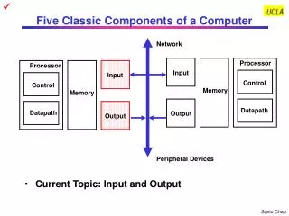
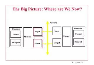
Implementing MIPS: the Fetch/Execute Cycle • High-level abstract view of fetch/execute implementation • use the program counter (PC) to read instruction address • fetch the instruction from memory and increment PC • use fields of the instruction to select registers to read • execute depending on the instruction • repeat…
Overview: Processor Implementation Styles • Single Cycle • perform each instruction in 1 clock cycle • clock cycle must be long enough for slowest instruction; therefore, • disadvantage: only as fast as slowest instruction • Multi-Cycle • break fetch/execute cycle into multiple steps • perform 1 step in each clock cycle • advantage: each instruction uses only as many cycles as it needs • Pipelined • execute each instruction in multiple steps • perform 1 step / instruction in each clock cycle • process multiple instructions in parallel – assembly line
Functional Elements • Two types of functional elements in the hardware: • elements that operate on data (called combinational elements) • elements that contain data (called state or sequential elements)
Combinational Elements • Works as an input output function, e.g., ALU • Combinational logic reads input data from one register and writes output data to another, or same, register • read/write happens in a single cycle – combinational element cannot store data from one cycle to a future one Combinational logic hardware units
State Elements • State elements contain data in internal storage, e.g., registers and memory • All state elements together define the state of the machine • What does this mean?Think of shutting down and starting up again… • Flipflops and latches are 1-bit state elements, equivalently, they are 1-bit memories • The output(s) of a flipflop or latch always depends on the bit value stored, i.e., its state, and can be called 1/0 or high/low or true/false • The input to a flipflop or latch can change its state depending on whether it is clocked or not…
Synchronous Logic: Clocked Latches and Flipflops • Clocks are used in synchronous logic to determine when a state element is to be updated • in level-triggered clocking methodology either the state changes only when the clock is high or only when it is low (technology-dependent) • in edge-triggered clocking methodology either the rising edge or falling edge is active (depending on technology) – i.e., states change only on rising edges or only on falling edge • Latchesare level-triggered • Flipflopsare edge-triggered
R e a d r e g i s t e r R e a d n u m b e r 1 d a t a 1 R e a d r e g i s t e r n u m b e r 2 R e g i s t e r f i l e W r i t e r e g i s t e r R e a d d a t a 2 W r i t e d a t a W r i t e State Elements on the Datapath: Register File • Registers are implemented with arrays of D-flipflops Clock 32 bits 5 bits 5 bits 5 bits 32 bits 32 bits Control signal Register file with two read ports and one write port
Clock Clock State Elements on the Datapath: Register File • Port implementation: Write port is implemented using a decoder – 5-to-32 decoder for 32 registers. Clock is relevant to write as register state may change only at clock edge Read ports are implemented with a pair of multiplexors – 5 bit multiplexors for 32 registers
Single-cycle Implementation of MIPS • Our first implementation of MIPS will use a single long clock cycle for every instruction • Every instruction begins on one up (or, down) clock edge and ends on the next up (or, down) clock edge • This approach is not practical as it is much slower than a multicycle implementation where different instruction classes can take different numbers of cycles • in a single-cycle implementation every instruction must take the same amount of time as the slowest instruction • in a multicycle implementation this problem is avoided by allowing quicker instructions to use fewer cycles • Even though the single-cycle approach is not practical it is simple and useful to understand first
Datapath: Instruction Store/Fetch & PC Increment Three elements used to store and fetch instructions and increment the PC Datapath
Animating the Datapath Instruction <- MEM[PC] PC <- PC + 4
Datapath: R-Type Instruction Two elements used to implement R-type instructions Datapath
Animating the Datapath add rd, rs, rt R[rd] <- R[rs] + R[rt];
Datapath: Load/Store Instruction Two additional elements used To implement load/stores Datapath
Animating the Datapath lw rt, offset(rs) R[rt] <- MEM[R[rs] + s_extend(offset)];
Animating the Datapath sw rt, offset(rs) MEM[R[rs] + sign_extend(offset)] <- R[rt]
Datapath: Branch Instruction No shift hardware required: simply connect wires from input to output, each shifted left 2 bits Datapath
Animating the Datapath beq rs, rt, offset • if (R[rs] == R[rt]) then PC <- PC+4 + s_extend(offset<<2)
MIPS Datapath I: Single-Cycle Input is either register (R-type) or sign-extended lower half of instruction (load/store) Data is either from ALU (R-type) or memory (load) Combining the datapaths for R-type instructions and load/stores using two multiplexors Fig. 5.11 Page 352
Animating the Datapath: R-type Instruction add rd,rs,rt
Animating the Datapath: Load Instruction lw rt,offset(rs)
Animating the Datapath: Store Instruction sw rt,offset(rs)
MIPS Datapath II: Single-Cycle Separate adder as ALU operations and PC increment occur in the same clock cycle Separate instruction memory as instruction and data read occur in the same clock cycle Adding instruction fetch
MIPS Datapath III: Single-Cycle New multiplexor Extra adder needed as both adders operate in each cycle Instruction address is either PC+4 or branch target address Adding branch capability and another multiplexor Important note: in a single-cycle implementation data cannot be stored during an instruction – it only moves through combinational logic Question: is the MemRead signal really needed?! Think of RegWrite…!
Datapath Executing add add rd, rs, rt
Datapath Executing lw lw rt,offset(rs)
Datapath Executing sw sw rt,offset(rs)
Datapath Executing beq beq r1,r2,offset
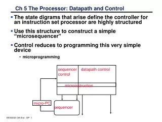
Control • Control unit takes input from • the instruction opcode bits • Control unit generates • ALU control input • write enable (possibly, read enable also) signals for each storage element • selector controls for each multiplexor
ALU Control • Plan to control ALU: main control sends a 2-bit ALUOp control field to the ALU control. Based on ALUOp and funct field of instruction the ALU control generates the 3-bit ALU control field • ALU control Func- fieldtion 000 and 001 or 010 add 110 sub 111 slt • ALU must perform • add for load/stores (ALUOp 00) • sub for branches (ALUOp 01) • one of and, or, add, sub, slt for R-type instructions, depending on the instruction’s 6-bit funct field (ALUOp 10) Recall from Ch. 4 2 3 ALUOp To ALU Main Control ALU Control ALU control input 6 Instruction funct field ALUOp generation by main control
ALUOp Funct field Operation ALUOp1 ALUOp0 F5 F4 F3 F2 F1 F0 0 0 X X X X X X 010 0 1 X X X X X X 110 1 X X X 0 0 0 0 010 1 X X X 0 0 1 0 110 1 X X X 0 1 0 0 000 1 X X X 0 1 0 1 001 1 X X X 1 0 1 0 111 Setting ALU Control Bits Instruction AluOp Instruction Funct Field Desired ALU control opcode operation ALU action input LW 00 load word xxxxxx add 010 SW 00 store word xxxxxx add 010 Branch eq 01 branch eq xxxxxx subtract 110 R-type 10 add 100000 add 010 R-type 10 subtract 100010 subtract 110 R-type 10 AND 100100 and 000 R-type 10 OR 100101 or 001 R-type 10 set on less 101010 set on less 111 *Typo in text Fig. 5.15: if it is X then there is potential conflict between line 2 and lines 3-7! * Truth table for ALU control bits
Designing the Main Control • Observations about MIPS instruction format • opcode is always in bits 31-26 • two registers to be read are always rs (bits 25-21) and rt (bits 20-16) • base register for load/stores is always rs (bits 25-21) • 16-bit offset for branch equal and load/store is always bits 15-0 • destination register for loads is in bits 20-16 (rt) while for R-type instructions it is in bits 15-11 (rd) (will require multiplexor to select) R-type opcode rs rt rd shamt funct 31-26 25-21 20-16 15-11 10-6 5-0 Load/store or branch opcode rs rt address 31-26 25-21 20-16 15-0
Datapath with Control I New multiplexor Adding control to the MIPS Datapath III (and a new multiplexor to select field to specify destination register): what are the functions of the control signals?
Control Signals Signal Name Effect when deasserted Effect when asserted RegDst The register destination number for the The register destination number for the Write register comes from the rt field (bits 20-16) Write register comes from the rd field (bits 15-11) RegWrite None The register on the Write register input is written with the value on the Write data input AlLUSrc The second ALU operand comes from the The second ALU operand is the sign-extended, second register file output (Read data 2) lower 16 bits of the instruction PCSrc The PC is replaced by the output of the adder The PC is replaced by the output of the adder that computes the value of PC + 4 that computes the branch target MemRead None Data memory contents designated by the address input are put on the first Read data output MemWrite None Data memory contents designated by the address input are replaced by the value of the Write data input MemtoReg The value fed to the register Write data input The value fed to the register Write data input comes from the ALU comes from the data memory Effects of the seven control signals
Datapath with Control II MIPS datapath with the control unit: input to control is the 6-bit instruction opcode field, output is seven 1-bit signals and the 2-bit ALUOp signal
PCSrc cannot be set directly from the opcode: zero test outcome is required Determining control signals for the MIPS datapath based on instruction opcode
Value depends on funct ??? Control Signals:R-Type Instruction 0 1 0 0 1 0 Control signals shown in blue 0
Control Signals:lw Instruction 0 010 0 0 1 1 1 Control signals shown in blue 1
Control Signals:sw Instruction 0 010 X 1 X 0 1 Control signals shown in blue 0
1 if Zero=1 Control Signals:beq Instruction 110 X 0 X 0 0 Control signals shown in blue 0
Datapath with Control III Jump opcode address 31-26 25-0 Composing jump target address New multiplexor with additional control bit Jump MIPS datapath extended to jumps: control unit generates new Jump control bit
R-type Instruction: Step 1add $t1, $t2, $t3 (active = bold) Fetch instruction and increment PC count
R-type Instruction: Step 2add $t1, $t2, $t3 (active = bold) Read two source registers from the register file
R-type Instruction: Step 3add $t1, $t2, $t3 (active = bold) ALU operates on the two register operands
R-type Instruction: Step 4add $t1, $t2, $t3 (active = bold) Write result to register
Implementation: ALU Control Block ALUOp Funct field Operation ALUOp1 ALUOp0 F5 F4 F3 F2 F1 F0 0 0 X X X X X X 010 0 1 X X X X X X 110 1 X X X 0 0 0 0 010 1 X X X 0 0 1 0 110 1 X X X 0 1 0 0 000 1 X X X 0 1 0 1 001 1 X X X 1 0 1 0 111 *Typo in text Fig. 5.15: if it is X then there is potential conflict between line 2 and lines 3-7! * Truth table for ALU control bits ALU control logic
Implementation: Main Control Block Signal R- lw sw beq name format Op5 0 1 1 0 Op4 0 0 0 0 Op3 0 0 1 0 Op2 0 0 0 1 Op1 0 1 1 0 Op0 0 1 1 0 RegDst 1 0 x x ALUSrc 0 1 1 0 MemtoReg 0 1 x x RegWrite 1 1 0 0 MemRead 0 1 0 0 MemWrite 0 0 1 0 Branch 0 0 0 1 ALUOp1 1 0 0 0 ALUOP2 0 0 0 1 Inputs Outputs Main control PLA (programmable logic array): principle underlying PLAs is that any logical expression can be written as a sum-of-products Truth table for main control signals