
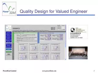
Quality Design for Valued Engineer
Quality Design for Valued Engineer. PowerESIM Features. PowerESIM Features. PowerESIM Features. PowerESIM Features. Agenda. 1 session - CBA concept & Loss charcteristic 2 session - General usage of poweresim 3 session - Loop analysis and MTBF 4 session - Xformer, thermal analysis.

Quality Design for Valued Engineer
E N D
Presentation Transcript
Agenda • 1 session - CBA concept & Loss charcteristic • 2 session - General usage of poweresim • 3 session - Loop analysis and MTBF • 4 session - Xformer, thermal analysis
What design engineer is doing R1 Vo Vin R2 Given Vo=0.5*Vin Rin=10 Pin=1@Vin=100 Given Vo=0.5*Vin Given Vo=0.5*Vin Rin=10 • Engineer Choice • R1=1, R2=1 • R1=10, R2=10 • R1=20, R2=20 • Engineer Choice • R1=5, R2=5 • Engineer Choice • R1=?, R2=?
Either less or more No. of Equations < No. of Variables No. of Equations = No. of Variables No. of Equations > No. of Variables
Making up equations Vi=100 Eqn 1 Vo=12 Eqn 2 Vo=Vi*D*Ns / (1-D)*Np Eqn 3 Np=? Eqn 4 Ns=? Eqn 5 Co=? Eqn6 Vds_max_M1=? Eqn7 Ids_max_M1=? Eqn8 IF_max_Do=? Eqn9 VR_max_Do=? Eqn10 Core_T1=? Eqn11 Wire_Np=? Eqn12 Wire_Ns=? Eqn13 T1 Do Vi Co Np Ns M1
Who is going to solve this? kth make up combination Vi=100 Eqn 1 Vo=12 Eqn 2 Vo=Vi*D*Ns / (1-D)*Np Eqn 3 Vi+Vo*Np/Ns=0.8Vds_max Eqn 4 Vo=Ns*0.3*fs/(1-D) Eqn 5 0.5*Vo_ripple=Q/Co Eqn6 Vds_max_M1=lowerest cost in stock Eqn7 Ids_max_M1=lowerest cost in stock Eqn8 IF_max_Do=2*Io Eqn9 VR_max_Do=1.2*(Vi*Ns/Np+Vo) Eqn10 Core_T1=recommended table from ferrite manufacturer Eqn11 Wire_Np=fully filled Eqn12 Wire_Ns=fully filled Eqn13
Can it be solved kth make up combination Vi=100 Eqn 1 Vo=12 Eqn 2 Vo=Vi*D*Ns / (1-D)*Np Eqn 3 Vi+Vo*Np/Ns=0.8Vds_max Eqn 4 Vo=Ns*0.3*fs/(1-D) Eqn 5 0.5*Vo_ripple=Q/Co Eqn6 Vds_max_M1=lowerest cost in stock Eqn7 Ids_max_M1=lowerest cost in stock Eqn8 IF_max_Do=2*Io Eqn9 VR_max_Do=1.2*(Vi*Ns/Np+Vo) Eqn10 Core_T1=recommended table from ferrite manufacturer Eqn11 Wire_Np=fully filled Eqn12 Wire_Ns=fully filled Eqn13 Solved Performance
Solving time to time Specification Expert Knowledge Equations solving Expert Knowledge Component selection Expert Knowledge Equations solving Component Traditional recursive iteration design flow
Component tier Component tier Component tier Result Result Result From serial to parallel Specification tier … Decision by Specification Proposed CBA Component Based Architecture
SPICE vs CBA CBA asking for SPICE asking for K Do Vi Co Np Rp Rp_ac Ns Rm Rs M1 Rs_ac
Result orientated – Thermal analysis Measured Simulated
Result orientated – Waveform analysis Measured Simulated
Result orientated – Loop Stability & Transient Measured Simulated
Result orientated – Input Current Harmonic Measured Simulated
Result orientated – MTBF & Life Time Measured Will be reported at 1/Mar/2100 Simulated
Result orientated – DVT report Measured Simulated
Build a Xformer Measured Lk=2.787uH Simulated Lk=2.982uH
MOSFET Loss Characteristics Gate drive Drain voltage Drain current t0 t1 t2 t3 t4 t0-t1 drain current catch up with load current t1-t2 drain voltage falling period t2-t3 MOSFET fully turn on t3-t4 drain voltage rising period with miller effect t4-t5 drain current falling period
Diode Loss Characteristics Ns Voltage Diode voltage Diode current t0 t1 t2 t3 t4 t5 t0-t1 diode in forward bias t1-t2 forward current drop to zero t2-t3 from zero current to peak reverse current (ta) t3-t4 reverse current droping period t4-t5 leakage current with reverse voltage
Rskin Rdc Rdc Rskin Ipri Isec Imag Rproximity Rfringe Rcore Xformer/Inductor Loss Characteristics • Rdc – wire dc losses • Rskin – wire skin effect losses • Rproximity – wire proximity effect losses • Rfringe – fringing flux losses • Rcore – core losses
Core Loss Characteristics – frequency and flux Loss Loss Loss=5W@0.2T Loss=3W@200kHz Loss=1W@0.1T Loss=1W@100kHz B Freq. • Every Engineer know, but . . .
Core Loss Characteristics – dc bias and duty cycle Loss Loss D Idc_bias Idc_bias • Higher Freq. higher loss • Higher flux change rate higher loss • Smaller D means higher flux change rate • Data sheet Loss is Idc_bias =0 • Large loss @ Idc_bias >Bs • Somewhere in between must exist rising slope @B D
Capacitor Loss Characteristics Irms ESR ESR ESR ESR=3@-25oC ESR=2@100Hz ESR=1@100kHz ESR=1@25oC Freq. Temp.
Phase margin m is the distance of the phase angle curve above - 180o at the cross over frequency ωc, where the magnitude plot crosses the 0db line. Gain Margin GM in db is the distance of the magnitude plot below the 0 db axis at the frequency where the phase is -180o. The Gain Margin and Phase Margin ensure stable operation ωc M(db) ω 0 GM m -180o ω First idea - Margins
Graphic averaging concept D Vin Averaged Thevin Rquivalent D Vin Vin*D
From non-linear to Laplace sL Vin*D(s) Vo(s) 1/sC sL Vin(s)*D Vo(s) 1/sC
ii ic Switching cell vo vi x More general approach – Inject-Absorbed-Current method Zp Variables concerned are the average values over one switching cycle. Absorbed current ii: ii = ii(x,vo,vi) (1) Injected current ic: ic= ic(x,vo,vi) (2)
Assuming it is a linear system • In differential form • In Laplace form
ii(s) ic(s) Cc Bi Yi(s) vi(s) vo(s) Zo(s) Zp(s) ia(s) iout(s) Ac Ai X(s) General graphical electrical model Output characteristic impedance
Ac(s) Bc(s) Cc(s) From non-linear to Laplace again
iL(s) b b vo = X = iL Loop 1 Loop 2 K - PWM H(s) H(s) + Current mode control Compensation network H(s) is to compensation a single pole, not a two pole LC network The inductor L becomes a controlled current source
Current mode control graphical model iL(s) Inductor current feedback Rs Current command - Fm d(s) + ve(s) + - Peak current mode control digital processor gain Vo(s) Output voltage feedback Input voltage feedback Vi(s)
Bc(s) Cc(s) Vi(s) + iL(s) + Zp(s) Vo(s) Ac(s) + d(s) Rs - Fm + ve(s) + - General graphical electrical model – include peak current mode control
Advanced option – subharmonic instability By introducing a second order (two pole) transfer function with resonate frequency at half of the switching frequency and a damping factor x,
More complicated graphical model Bc(s) Cc(s) Vi(s) + iL(s) + Zp(s) F(s) Vo(s) Ac(s) + d(s) Rs - Fm + ve(s) + -
Advance vs Ordinary Modified by F(s) Modified by F(s)
Continued mode operation and Discontinued mode operation Voltage mode, Peak current mode and Averaged current mode Parasistic effect Compensation method After all, it should be completed by a program and once forever! Advance and More advance
After all, you only need a final compensated design Automatic compensation


![[PDF] Prepare for ASQ Software Quality Engineer (CSQE) Certification](https://cdn4.slideserve.com/8456348/how-to-prepare-for-asq-csqe-certification-dt.jpg)