LC-3 Computer Architecture: Machine Instructions and Programming
250 likes | 268 Vues
Explore LC-3 Computer Architecture, Machine Instructions, and Programming Techniques in Machine and Assembly Language. Learn about addressing modes, instruction formats, and program execution cycles.

LC-3 Computer Architecture: Machine Instructions and Programming
E N D
Presentation Transcript
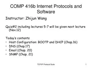
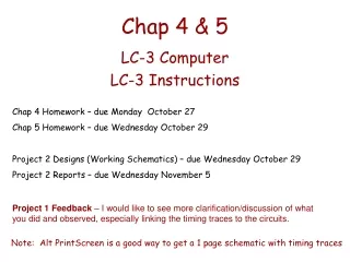
Chap 4 & 5 Chap 4 Homework – due Monday October 27 Chap 5 Homework – due Wednesday October 29 Project 2 Designs (Working Schematics) – due Wednesday October 29 Project 2 Reports – due Wednesday November 5 LC-3 Computer LC-3 Instructions Project 1Feedback – I would like to see more clarification/discussion of what you did and observed, especially linking the timing traces to the circuits. Note: Alt PrintScreen is a good way to get a 1 page schematic with timing traces
Chapters 4 & 5: The LC-3 Computer LC-3 Computer Architecture Machine Instructions Programming in Machine Language (Binary or Hex Code) (One word per instruction) Programming in Assembly Language (Symbolic Code) (One statement per instruction) LC-3 Editor & Simulator Go to: http://www.mhhe.com/patt2 Download: LC-3 Simulator (Either Windows or Unix version) Simulator Download includes LC-3 (Simulator) & LC-Edit Download: Simulator Lab Manual
LC-3 Memory Map (64K of 16 bit words) 256 words 256 words 23.5 K words 39.5 K words 512 words
The LC-3 Computeravon Neumannmachine • The Instruction Cycle • Fetch: Next Instruction from Memory • (PC) (points to) next instruction • PC (PC) + 1 • Decode: Fetched Instruction • Evaluate: Instr &Address (es) • (find where the data is) • Fetch: Operand (s) • (get data as specified) • Execute: Operation • Store: Result • (if specified) PSW Memory PSW (Program Status Word): Bits: 15 10 9 8 2 1 0 | S| |Priority| | N| Z| P|
Computer Machine Instruction Formats • What is IN an instruction? • Operation code – what to do • Input Operand(s) – where to get input operands (memory, registers) • Output Operand(s) – Where to put results (memory, registers) • What are the major instruction types? • Data Movement (load, store, etc.) • Operate (add, sub, mult, OR, AND, etc.) • Control (branch, jump to subroutine, etc.)
The LC-3 Instruction Addressing Modes • Register (Operand is in one of the 8 registers) • Immediate (Operand is in the instruction) • PC-relative (Operand is “offset” from the (PC) ) • Indirect (The “Operand” actually points to the real Operand • – rather than being the operand) • Base + Offset (Base relative)(Operand is “offset” from the • contents of a register) • Note: no Direct Addressing defined in the LC-3
LC-3 Instructions (Fig 5.3 – Appendix a) • Addressing Modes • Register • (Operand is in one of the 8 registers) • PC-relative • (Operand is “offset” from where the PC points) • Base + Offset (Base relative) • (Operand is “offset” from the contents of a register) • Immediate • (Operand is in the instruction) • Indirect • (The “Operand” points to the real address of Operand • – rather than being the operand)
Operate Instructions • Only three operate Instructions: ADD, AND, NOT • Source and Destination operands are: Registers
NOT (Register) Note: Src and Dstcould be the same register.
ADD/AND (Immediate) Note: Immediate field issign-extended to 16 bits.
Data Movement Instructions • Load - read data from memory to register • LD: PC-relative mode [0010 DR PCoffset9] • LDI: indirect mode [1010 DR PCoffset9] • LDR: base+offset mode [0110 DR BaseR offset6] • Store - write data from register to memory • ST: PC-relative mode [0011 DR PCoffset9] • STI: indirect mode [1011 DR PCoffset9] • STR: base+offset mode [0111 DR BaseR offset6] • Load effective address – address saved in register • LEA: immediate mode [1110 DR PCoffset9]
Branch Instruction BR [0000 nzp PCoffset9] • Branch specifies one or more condition codes Program Status Word (PSW): Bits: 15 10 9 8 2 1 0 | S| |Priority| |N|Z|P| • If the set bit is specified, the branch is taken: • PC is set to the address specified in the instruction - Target address is made by adding SEXT(IR[8:0]) to the PC • If the branch is not taken: - the next sequential instruction (PC) is executed.
BR + SEXT
Jump Instruction JMP BaseR [1100 000 BaseR 000000] • Jump is an unconditional branch -- always taken. • BaseR • Address is contents of the register • Allows any target address.
Example LC-3 Program • Write a program to add 12 integers and store the result in a Register.
Compute the Sum of 12 Integers Program • Program begins at location x3000. • Integers begin at location x3100. R1 x3100R3 0 (Sum)R2 12(count) R2=0? R4 M[R1] R3 R3+R4R1 R1+1 R2 R2-1 NO YES R1: “Array” index pointer (Begin with location 3100) R3: Accumulator for the sum of integers R2: Loop counter (Count down from 12) R4: Temporary register to store next integer
Sum integers from x3100 – x310B R1: “Array” index pointer (Begin with location 3100) R3: Accumulator for the sum of integers R2: Loop counter (Count down from 12) R4: Temporary register to store next integer