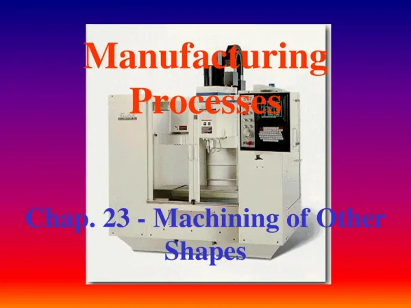
Manufacturing Processes
Explore the atomic structure of materials, periodic table elements, bonding between atoms and molecules, and their impact on material properties. Understand the basics of electricity, stability, and bonding types.

Manufacturing Processes
E N D
Presentation Transcript
Manufacturing Processes Chapter 2: Materials Properties Dr. Yazan Al-Zain Department of Industrial Engineering University of Jordan, Amman-Jordan
Introduction • Some materials are hard and some are soft. Some are brittle while others are ductile. Some materials can withstand temperature while others cannot. • The reason for these differences between various materials is strongly related to the atomic structure; the way the atoms are arranged within the materials. It is also related to the interactions that exist among the constituent atoms or molecules. • The understanding of the atomic structure of materials allows us to predict and evaluate their properties.
Atomic Structure & The Elements • The atom is the basic structural unit of matter. It is composed of a small nucleus composed of protons and neutrons, which is encircled by moving electrons. • Both electrons and protons are electrically charged, the charge magnitude being 1.60 10-19 C, which is negative in sign for electrons and positive for protons; neutrons are electrically neutral. • Protons and neutrons have approximately the same mass, 1.67 10-27 kg, which is significantly larger than that of an electron, 9.11 10-31 kg. • The number of electrons (or protons) identifies the atomic number (Z) and the element of the atom. (Z= 1 & 90 for H and U, respectively).
Atomic Structure & The Elements • The elements are grouped into families and relationships established between and within the families by means of the periodic table. • Grouped into metals, nonmetals and intermediate (metalloids or semimetals). • Depending on temp. & press. All these elements can exist as liquid, solid and gas; e.g. at room temp.: Fe: Metal Hg: Liquid. N: gas. Fig. 2-1: The periodic table.
Atomic Structure & The Elements • In the periodic table, elements are arranged in such a way that similarities exist between elements in the same columns; for example: • Noble gases: found in the extreme right column (He, Ne, Ar, Kr, Xe & Rn) are chemically stable and exhibit low reaction rates. • The halogens: found in column VIIA (F, Cl, Br, I & At) share similar properties. • The noble metals: found in column IB (Cu, Ag & Au) share similar properties.
Atomic Structure & The Elements • Many of the similarities and differences between elements can be explained by their respective atomic structures. • The planetary model (Bohr atom): the simplest atomic model showing the electrons of the atom orbiting around the nucleus at certain fixed distance, called shells. Fig. 2-2: Planetary (Bohr) atomic model.
Atomic Structure & The Elements • The maximum numbers of atoms / orbit can be defined as: - Max. no. of electrons / orbit = 2n2; where n identifies the orbit. • The electrons in the outmost shell are called valance electrons; the number of these atoms determine the atom’s chemical affinity for other atoms. • For example, Max. no. of electrons for the first orbit is 2. Hydrogen atom has one electron and hence needs another electron in its shell to become stable. That’s why H reacts (bonds) readily with other atoms such as O to form H2O or with another H atom to form H2 molecule. • On the other hand, the two electrons in the helium’s atom only orbit are the maximum allowed, and so He is very stable.
Bonding Between Atoms & Molecules • Atoms are bonded together to form molecules. Molecules on the other hand attract to each other to form other bonds, relatively weaker that the atom-atom bonds. Thus, we have two types of bonding; primary and secondary bonds. (1) Primary bonds: characterized by strong atom-to-atom attractions that involve the exchange of valence electrons. Primary bonds include the following forms: • Ionic bonds: in this form, the atoms of one element give up their outer electron(s), which are in turn attracted to atoms of some other element to increase their electron count in the outmost shell to 8. • For example, the bond between fluorine and sodium. Note: properties of solid materials with ionic bonding include low electrical conductivity and poor ductility. Fig. 2-3: Sodium fluoride molecule (ionic bond).
Bonding Between Atoms & Molecules (1) Primary bonds: characterized by strong atom-to-atom attractions that involve the exchange of valence electrons. Primary bonds include the following forms: (b)Covalent bonds: is one in which electrons are shared between atoms in their outmost shells to achieve a stable set of eight. • For example, a fluorine atom bonds to another fluorine atom to form fluorine gas F2. Also, one carbon atom (4 electrons in the outmost shell) bonds with four hydrogen atoms (only one electron in the only shell) to form methane gas. Note: Ionic and covalent bonds are called intramolecular bonds because they involve attractive forces between atoms within the molecule. Fig. 2-4: Methane molecule (covalent bond).
Bonding Between Atoms & Molecules (1) Primary bonds: characterized by strong atom-to-atom attractions that involve the exchange of valence electrons. Primary bonds include the following forms: (c)Metallic bonds: involve the sharing of outer-shell electrons by all atoms to form a general electron cloud (sea of electrons) that permeates the entire block . This cloud provide the attractive forces to hold the atoms together and form a strong, rigid structure. • For example, bonds in pure metals and metal alloys. Note: Because of the general sharing of electrons, and their freedom to move within the metals, metallic bonding provides for good electrical conductivity. Materials with this type of bonding have good ductility, and good heat induction. Fig. 2-5: metallic bonding.
Bonding Between Atoms & Molecules (2) Secondary bonds: involve interaction forces between molecules, or intermolecular forces. There is no transfer or sharing of electrons in secondary bonding, and those bonds are therefore weaker than the primary bond. There are three forms of secondary bonds: (a)Dipole forces: arise in a molecule comprising 2 atoms that have equal and opposite electrical charges. Each molecule therefore forms a dipole. • For example, bonds between two HCl molecules. Fig. 2-6: dipole forces.
Bonding Between Atoms & Molecules (2) Secondary bonds: involve interaction forces between molecules, or intermolecular forces. There is no transfer or sharing of electrons in secondary bonding, and those bonds are therefore weaker than the primary bond. There are three forms of secondary bonds: (b)London forces: involve attractive forces between nonpolar molecules; that is, the atoms in the molecule do not form dipoles in the same sense as dipole forces. However, owing to the rapid motion of electrons in orbit around the molecule, temporary dipoles form when more electrons happen to be on one side of the molecule than the other. Note: Dipole and London forces are often referred to as van der Waals forces. Fig. 2-7: London forces.
Bonding Between Atoms & Molecules (2) Secondary bonds: involve interaction forces between molecules, or intermolecular forces. There is no transfer or sharing of electrons in secondary bonding, and those bonds are therefore weaker than the primary bond. There are three forms of secondary bonds: (c)Hydrogen bonding: occurs in molecules containing H atoms that are covalently bonded to another atom (e.g. oxygen in H2O). Since the electrons needed to complete the shell of the hydrogen atom are aligned on one side of its nucleolus, the opposite side has a net positive charge that attracts the electrons of atoms in neighboring molecules. Note: hydrogen bonding is generally stronger than the other forms of secondary bonding (dipole and London forces), and it is important in the formation of many polymers. Fig. 2-8: Hydrogen bonding (water).
Crystalline Structures • A crystalline material is one in which the atoms are situated in a repeating or periodic array over large atomic distances; that is, long-range order exists, such that upon solidification, the atoms will position themselves in a repetitive three-dimensional pattern, in which each atom is bonded to its nearest-neighbor atoms (that includes all metals, many ceramics and many polymers). • For those that do not crystallize, this long-range atomic order is absent; these are called amorphous materials. • In metals, three lattice structures are common: (1) body-centered cubic, (2) face-centered cubic and (3) hexagonal close-packed.
Crystalline Structures Fig. 2-9: BCC crystal structure. (1) BCC: a crystal structure that has a cubic unit cell with atoms located at all eight corners and a single atom at the cube center (total of two atoms/unit cell). Center and corner atoms touch one another along cube diagonals. Coordination number and atomic packing factor for BCC are 8 and 0.68, respectively.
Crystalline Structures (2) FCC: a crystal structure that has a cubic unit cell with atoms located at all eight corners and six atoms at the center of each face of the cube. (total of four atoms/unit cell). Atoms touch one another across a face diagonal. a = 2r √2; where a is the lattice constant and r is the atomic radius. Coordination number and atomic packing factor for FCC are 12 and 0.74, respectively. So, what do the Coordination number and atomic packing factor mean?? Fig. 2-10: FCC crystal structure.
Crystalline Structures • Coordination number: the number of nearest-neighbor atoms per atom. • For FCC, the coordination number is 12; the front face atom has four corner nearest-neighbor atoms surrounding it, four face atoms that are in contact from behind, and four other equivalent face atoms residing in the next unit cell to the front. • For the BCC, the coordination number is 8; each center atom has as nearest neighbors as its eight corner atoms.
Crystalline Structures • Atomic packing factor (APF): is the fraction of solid sphere volume in a unit cell, assuming the atomic hard sphere model. • APF = Volume of atoms in a unit cell / Volume if unit cell. • Calculate the APF for FCC lattice.
Crystalline Structures Fig. 2-11: HCP crystal structure. (3) HCP: the top and bottom faces of the unit cell consist of six atoms that form regular hexagons and surround a single atom in the center. Another plane that provides three additional atoms to the unit cell is situated between the top and bottom planes. The equivalent of six atoms is contained in each unit cell; one-sixth of each of the 12 top and bottom face corner atoms, one-half of each of the 2 center face atoms, and all the 3 midplane interior atoms. If a and c represent, respectively, the short and long unit cell dimensions, the c/a ratio should be 1.633; however, for some HCP metals this ratio deviates from the ideal value. Coordination number and atomic packing factor for HCP is similar to those of FCC (12 and 0.74, respectively).
Imperfections in Crystals • Usually, crystal structures are not perfect. The imperfections (defects) arise due to the inability of the solidifying material to continue the replication of the unit cell indefinitely without interruption (grain boundaries are an example). • In some other cases, these imperfections are introduced purposely during the manufacturing process; e.g. the addition of an alloying element in a metal to increase its strength (C in Fe). • Hence, either term, imperfections or defects refers to the deviation in the regular pattern of the crystalline lattice structure. These can be catalogued as: (1) point defects, (2) line defects, and (3) surface defects.
Imperfections in Crystals • Point Defects: there are four types of point defects: (a) The simplest of the point defects is a vacancy, or vacant lattice site, one normally occupied from which an atom is missing. (b) Ion-pair vacancy (or Schottky defect) involves a missing pair of ions of opposite charge in a compound that has an over all charge balance. (c) Interstitialcy: a lattice distortion produced by the presence of an extra atom in the structure. (d) Displaced ion: (Frenkel defect) occurs when an ion becomes removed from a regular position in the lattice structure and inserted into an interstitial position not normally occupied by such an ion.
Imperfections in Crystals Vacancy Interstitialcy Ion-pair vacancy Frenkel defect Fig. 2-12: Various types of point defects.
Imperfections in Crystals (2) Line Defects: a line defect is a connected group of point defects that form a line in the lattice structure. The most important line defect is the dislocation, which can take two forms: (a) Edge dislocation: an extra portion of a plane of atoms, or half-plane, the edge of which terminates within the crystal. it is a linear defect that centers around the line that is defined along the end of the extra half-plane of atoms. This is sometimes termed the dislocation line, which, for the edge dislocation in Figure 2-13, is perpendicular to the plane of the page. Note: lattice distortion is maximum near the dislocation line. Fig. 2-13: Edge dislocation.
Imperfections in Crystals (2) Line Defects: a line defect is a connected group of point defects that form a line in the lattice structure. The most important line defect is the dislocation, which can take two forms: (b) Screw dislocation: which may be thought of as being formed by a shear stress that is applied to produce the distortion shown in Figure 2-14: the upper front region of the crystal is shifted one atomic distance to the right relative to the bottom portion. Note: both types of dislocations are usually found in materials. They arise during solidification processes (casting) or during deformation processes (metal forming). Fig. 2-14: Screw dislocation.
Imperfections in Crystals Fig 2-15: A transmission electron micrograph of a titanium alloy in which the dark lines are dislocations. 51,450. (Courtesy of M. R. Plichta, Michigan Technological University.)
Imperfections in Crystals (3) Surface Defects: imperfections that extend in two directions to form a boundary. • The most obvious example is (a) the external surface of a crystalline object that defines its shape. The surface is an interruption in the lattice structure. • Surface boundaries can also lie inside the material. Grain boundaries are the best example of these (b) internal surface interruptions.
Deformation in Metallic Crystals • When a crystal is subjected to gradually increasing mechanical stress, its initial response it deform elastically (elastic deformation). If the stress reaches a high value relative to the electrostatic forces holding the atoms in their lattice positions, a permanent shape change occurs, called plastic deformation. (1) Elastic deformation: that type of deformation where the lattice structure is being tilted without any changes of position among the atoms in the lattice (Fig. 2-16 a and b). If the force is removed, the lattice structure (and therefore the crystal) returns to its original shape. Fig. 2-16: (a) original crystal (b) elastic deformation (c) plastic deformation .
Deformation in Metallic Crystals • When a crystal is subjected to gradually increasing mechanical stress, its initial response it deform elastically (elastic deformation). If the stress reaches a high value relative to the electrostatic forces holding the atoms in their lattice positions, a permanent shape change occurs, called plastic deformation. (2) Plastic deformation: that type of deformation where the atoms in the lattice have permanently moved from their previous locations, and a new equilibrium lattice has been formed (Fig. 2-16 c). If the force is removed, the lattice structure (and therefore the crystal) does not return to its original shape. Fig. 2-16: (a) original crystal (b) elastic deformation (c) plastic deformation .
Deformation in Metallic Crystals • Plastic deformation: the lattice deformation shown in (c) is one possible mechanism called slip, by which plastic deformation can occur in a crystalline structure. The other is called twinning. • Slip and slip systems: slip involves the movement of atoms on the opposite sides of a plane in the lattice (preferred plane), and in that plane there are specific directions along which dislocation motion occurs. This plane is called the slip plane; it follows that the direction of movement is called the slip direction. This combination of the slip plane and the slip direction is termed the slip system (different crystal structures have different slip systems). The slip system depends on the crystal structure of the metal and is such that the atomic distortion that accompanies the motion of a dislocation is a minimum. Materials with dislocations deform much more rapidly than in a perfect structure. Dislocations move with stress. Easier to move a dislocation than it is to deform the lattice itself! Why??
Deformation in Metallic Crystals • The atoms at the edge dislocation require a smaller displacement within the distorted lattice structure in order to reach a new equilibrium position. Thus, a lower energy is needed to realign the atoms into the new positions than if the lattice were missing a dislocation. Fig. 2-17: Atomic rearrangements that accompany the motion of an edge dislocation as it moves in response to an applied shear stress. (a) The extra half-plane of atoms is labeled A. (b) The dislocation moves one atomic distance to the right as A links up to the lower portion of plane B; in the process, the upper portion of B becomes the extra half-plane. (c) A step forms on the surface of the crystal as the extra half-plane exits.
Deformation in Metallic Crystals; Slip Systems in FCC, BCC Fig. 2-18: (a) A {111} <110> slip system shown within an FCC unit cell. (b) The (111) plane from (a) and three <110> slip directions (as indicated by arrows) within that plane comprise possible slip systems. There are 12 slip systems: four unique {111} planes and, within each plane, three independent <110> directions. BCC crystal structure has more slip systems than FCC, an example is: {110} <111>.
Deformation in Metallic Crystals • Plastic deformation: the lattice deformation shown in (c) is one possible mechanism called slip, by which plastic deformation can occur in a crystalline structure. The other is called twinning. • Twinning: it is another way in which metal crystals plastically deform. Twinning is the mechanism of plastic deformation in which atoms of one side of a plane (twinning plane) are shifted to form a mirror image of the other side of the plane. Twinning is important for HCP metals as they do not slip readily. Rate of deformation: slip needs time while twinning occurs instantaneously. Fig. 2-19: Twinning involves the formation of an atomic mirror image (i.e., a “twin”) on the opposite side of the twinning plane (a) before, and (b) after twinning. When subjected to high deformation rates, some metals would twin, while at moderate rates they deform by slip.
Grains and Grain Boundaries (GBs) • Most crystalline solids are composed of a collection of many small crystals or grains; such materials are termed polycrystalline. Various stages in the solidification of a polycrystalline specimen are represented schematically in Fig. 2-20. Initially, small crystals or nuclei form at various positions. These have random crystallographic orientations, as indicated by the square grids. The small grains grow by the successive addition from the surrounding liquid of atoms to the structure of each. The extremities of adjacent grains impinge on one another as the solidification process approaches completion. As indicated in the figure, the crystallographic orientation varies from grain to grain. Also, there exists some atomic mismatch within the region where two grains meet; this area, called a grain boundary. Fig. 2-20: Schematic diagrams of the various stages in the solidification of a polycrystalline material; the square grids depict unit cells. (a) Small crystallite nuclei. (b) Growth of the crystallites; the obstruction of some grains that are adjacent to one another is also shown. (c) Upon completion of solidification, grains having irregular shapes have formed. (d) The grain structure as it would appear under the microscope; dark lines are the grain boundaries.
Grains and Grain Boundaries (GBs) Grain size is inversely related to cooling rate. Grain size is important in metals; it affects the properties. Materials with small grain sizes have higher strength and hardness (GBs hinder dislocation motion).
Noncrystalline (Amorphous)Structures • Noncrystalline solids are those materials that lack a systematic and regular arrangement of atoms over relatively large atomic distances. Sometimes such materials are also called amorphous (meaning literally without form), or supercooled liquids, inasmuch as their atomic structure resembles that of a liquid; e.g. many glasses, and rubber. • Amorphous structures can form if the cooling rate during the transformation from liquid to solid is high enough, so that little time is allowed for the ordering process. Fig 2-21: Two-dimensional schemes of the structure of (a) crystalline and (b) noncrystalline SiO2.
Noncrystalline (Amorphous)Structures • There are two main differences between crystalline and noncrystalline materials: • Absence of a long-range order in the molecular structure of a noncrystalline material (as shown in the previous figure). • Differences in melting and thermal expansion characteristics. Due to thermal expansion Fig 2-22: Change in volume for pure metal vs. glass. Tg: temp. at which the supercooled liquid converts to solid. Tm: melting temp. of the metal.
Engineering Materials • Metals: - Crystalline (BCC, FCC, HCP, etc). – Metallic bonding. Structure and bonding make metals strong, hard, ductile, high thermal and electrical conductivity, opaqueness and reflectivity. • Ceramics: - Mostly crystalline. – Ionic or covalent bonding, or both. – High hardness and stiffness. – Brittleness. – Electrical and thermal insulating, and chemically inert. • Polymers: A polymer molecule consists of many repeating mers to form very large molecules held together by covalent bonding. Secondary bonding (van der Waals) holds the molecules together. – Low density. – High electrical resistivity. – Low thermal conductivity. – Some polymers are hard and rigid while other exhibit great elasticity. - Amorphous or amorphous and crystalline. – Three types: (a) Thermoplastic polymers. (b) Thermosetting polymers, and (c) Elastomers.