Polyimide memory: a pithy guideline for future applications
200 likes | 379 Vues
Advisor : Professor Guey-Sheng Liou Reporter : Ming-Chi Tsai Date : 2013/11/15. Polyimide memory: a pithy guideline for future applications. J. Mater. Chem. C, 2013 , 1 , 7623-7634, G. S. Liou * et al. Introduction Experiment Results and Discussion Summary. Outline.

Polyimide memory: a pithy guideline for future applications
E N D
Presentation Transcript
Advisor : Professor Guey-ShengLiou Reporter: Ming-Chi Tsai Date : 2013/11/15 Polyimide memory: a pithy guideline for future applications J. Mater. Chem. C, 2013, 1, 7623-7634, G. S. Liou* et al.
Introduction Experiment Results and Discussion Summary Outline
Polymer memory devices • Advantages : • Low cost • Solution processability • Flexibility • 3D stacking device • Polyimide is one of the most suitable material for memory • Thermal stability • Chemical resistance • Mechanical strength
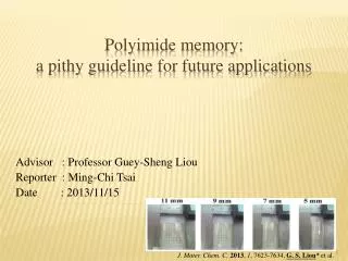
Fabrication process of Polymer memory devices J. Mater. Chem. C, 2013, 1, 7623-7634, G. S. Liou* et al.
Principle 1st sweep : 0~4V an abrupt increase in current observed at 3.2V (writing) 2nd sweep : 0~4V (reading) 3rd sweep : 0~-4V an abrupt decrease in current observed at -2.1V (erasing) 4th sweep : 0~-4V OFF state 5th sweep : 0~4V (rewriting) 6th sweep : 0~4V (reading) 7th sweep : 0~4V turn off external power 1 min device turned off (erasing) and (rewriting) 8th sweep : (reading) Memory type : DRAM J. Am. Chem. Soc., 2006, 128, 8732-8733, En-Tang Kang* et al.
Principle • Field induced CT theory • Conformational change • LUMO Energy level • Dipole moment • Large conjugation J. Am. Chem. Soc., 2006, 128, 8732-8733, En-Tang Kang* et al.
Polyimide synthesis • One-step polycondensation • Two-step polycondensation ShahramMehdipour-Ataei*, et al., Iranian Polymer Journal,2008, 17,95-124
Volatile DRAM and SRAM properties 1st sweep : 0~5V 2.7V (writing) 2nd sweep : 0~5V (reading) 3rd sweep : 0~-2V -0.9V (erasing) 4th sweep : 0~-2V OFF state 5th sweep : 0~5V (rewriting) 6th sweep : 0~5V (reading) 7th sweep : 0~5V power off 1 min (erasing) and (rewriting) 8th sweep : (reading) Memory type : DRAM 3rd sweep : 0~-6V-0.9V (erasing) -2.3V (writing) Can be written bidirectionally J. Appl. Phys., 2009, 105, 044501, En-Tang Kang* et al.
Volatile DRAM and SRAM properties Good stability when operated time 1st sweep : 0~4V 2.3V (writing) 2nd sweep : 0~4V (reading) 3rd sweep : 0~-4V (reading) nonerasable 4th sweep : 0~-4V power off 4 mins (rewriting) 5th sweep : 0~-4V (reading) 6th sweep : 0~-4V power off 4 mins (rewriting) Memory type : SRAM Chem. Mater., 2009, 21, 3391–3399, En-Tang Kang* et al.
Volatile DRAM and SRAM properties PI → PA DARM → SRAM J. Mater. Chem., 2012, 22, 14085, G. S. Liou* et al.
Volatile DRAM and SRAM properties • PA (SARM device) • Block the occurring of back CT • Higher dipole moment • More nonplanar • Lower switching on voltage -3.3V • Higher HOMO energy level • Fewer intermediate LUMOs Stability test Both PI and PA memory devices are stability when operating
Non-volatile FLASH and WORM type memory properties Take APTT-6FDA for example 1st sweep : 0~4V 1.6V (writing) 2nd sweep : 0~4V power off 10 mins (reading) 3rd sweep : 0~-6V (reading & erasing) -3.2V 4th sweep : 0~-6V OFFstate 5th sweep : 0~4V (rewriting) 6th sweep : 0~-4V power off 10 mins (reading) Memory type : Flash memory Macromolecules,2009, 42, 4456–4463, Mitsuru Ueda*, W. C. Chen* et al
Non-volatile FLASH and WORM type memory properties • Write Once Read Many times (WORM) • Nonerasable • Highest dipole moment J. Mater. Chem., 2012, 22, 14085, G. S. Liou* et al.
Non-volatile FLASH and WORM type memory properties From Volatile to Nonvolatile by PeryleneDiimideComposition in Random Copolymer Acceptor Donor The (PBI-0, PBI-1, PBI-2.5) and (PBI-5, PBI-10) devices provided volatile and nonvolatile WORM behavior, respectively. Macromolecules, 2012, 45, 4556, Mitsuru Ueda*, W. C. Chen*, C. L. Liu* et al.
Summary 3D structure (192 cells) In future application of PI as a good memory device material Flexible • Devices structure and operating mechanism of the memory device is quite simple • Low processing cost • Show extremely high endurance during long term operation
