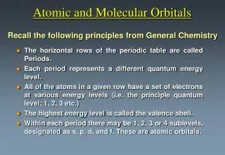
Atomic Orbitals
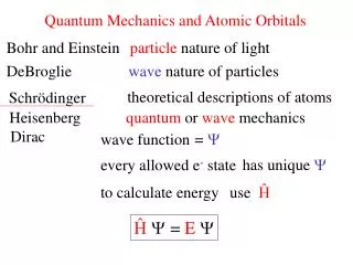
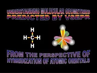
Atomic Orbitals. s -orbitals. p -orbitals. d -orbitals. H B. H A. H A - H B. = H 2. Chemical Bonding. Overlap of half-filled orbitals - bond formation. Formation of Molecular Hydrogen from Atoms. Overlap of filled orbitals - no bonding. Periodic Chart. Crystal Bonding.

Atomic Orbitals
E N D
Presentation Transcript
Atomic Orbitals s-orbitals p-orbitals d-orbitals
HB HA HA - HB = H2 Chemical Bonding Overlap of half-filled orbitals - bond formation Formation of Molecular Hydrogen from Atoms Overlap of filled orbitals - no bonding
Crystal Bonding sp3 antibonding orbitals sp3 bonding orbitals Silicon Crystal Bonding
Semiconductor Band Structures Silicon Germanium Gallium Arsenide
Intrinsic Semiconductor Aggregate Band Structure Fermi-Dirac Distribution
n-type Semiconductor Aggregate Band Structure Donor Ionization Fermi-Dirac Distribution
p-type Semiconductor Aggregate Band Structure Acceptor Ionization Fermi-Dirac Distribution
Temperature Dependence Fermi level shift in extrinsic silicon Mobile electron concentration (ND= 1.15(1016) cm3)
No Field Field Present Pictorial representation of carrier trajectory Carrier Mobility Carrier drift velocity vs applied field in intrinsic silicon
Effect of Dopant Impurities Effect of total dopant concentration on carrier mobility Resistivity of bulk silicon as a function of net dopant concentration
Diamond Cubic Lattice a = lattice parameter; length of cubic unit cell edge Silicon atoms have tetrahedral coordination in a FCC (face centered cubic) Bravais lattice
z z z y y y x x x Miller Indices 100 110 111
Diamond Cubic Model 100 110 111
Cleavage Planes Crystals naturally have cleavage planes along which they are easily broken. These correspond to crystal planes of low bond density. In the diamond cubic structure, cleavage occurs along 110 planes.
Czochralski Process Equipment Image courtesy Microchemicals
CZ Growth under Rapid Stirring Distribution Coefficients CZ Dopant Profiles under Conditions of Rapid Stirring
Zone Refining Si Ingot Heater Ingot slowly passes through the needle’s eye heater so that the molten zone is “swept” through the ingot from one end to the other
Multiple Pass FZ Process Almost arbitrarily pure silicon can be obtained by multiple pass zone refining.
“Dangling Bonds” Vacancy (Schottky Defect)
Dislocations Edge Dislocation Screw Dislocation
Burgers Vector Edge Dislocation Screw Dislocation Dislocations in Silicon [100] [111]
Stacking Faults Intrinsic Stacking Fault Extrinsic Stacking Fault
Vacancy-Interstitial Equilibrium Formation of a Frenkel defect - vacancy-interstitial pair “Chemical” Equilibrium
Thermodynamic Potentials E = Internal Energy H = Enthalpy (heat content) A = Helmholtz Free Energy G = Gibbs Free Energy For condensed phases: E and H are equivalent = internal energy (total system energy) A and G are equivalent = free energy (energy available for work) T = Absolute Temperature S = Entropy (disorder) Boltzmann’s relation
Internal Gettering Gettering removes harmful impurities from the front side of the wafer rendering them electrically innocuous. High temperature anneal - denuded zone formation Low temperature anneal - nucleation Intermediate temperature anneal - precipitate growth
Precipitate Free Energy a) - Free energy of formation of a spherical precipitate as a function of radius b) - Saturated solid solution of B (e.g., interstitial oxygen) in A (e.g., silicon crystal) c) - Nucleus formation
Substrate Characterization by XRD Bragg pattern - [hk0], [h0l], or [0kl]
Wafer Finishing Ingot slicing into raw wafers Schematic of chemical mechanical polishing
Vapor-Liquid-Solid (VLS) Growth Si nanowires grown by VLS (at IBM)
liquid A B solid Gold-Silicon Eutectic A – eutectic melt mixed with solid gold B – eutectic melt mixed with solid silicon
Non-bridging oxygen SiO4 tetrahedron Silanol Silicon Dioxide Network
Thermal Oxidation One dimensional model of oxide growth Deal-Grove growth kinetics
Oxidation Kinetics Rate constants for wet and dry oxidation on [100] and [111] surfaces
Linear Rate Constant Orientation dependence for [100] and [111] surfaces affects only the “pre-exponential” factor and not the activation energy