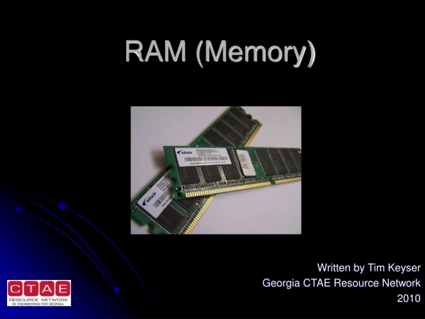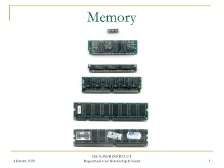
Memory (RAM) Organization
Memory (RAM) Organization. Each location is addressable Addresses are binary numbers Addresses used at different granularities each bit is possible, but not very likely each byte is possible, but seldom used (today) typical usage is a “word” of memory

Memory (RAM) Organization
E N D
Presentation Transcript
Memory (RAM) Organization • Each location is addressable • Addresses are binary numbers • Addresses used at different granularities • each bit is possible, but not very likely • each byte is possible, but seldom used (today) • typical usage is a “word” of memory • Each CPU designed with a particular word size (e.g. 8-bit, 16-bit, 32-bit, 64-bit)
Memory • Latches: 1-bit memory circuits • SR latch (S=Set, R=Reset) • Set/Reset control signals • Memory value and its complement as outputs • D latch (D = Data) • like SR, but avoids problem of S = R = 1 • S comes from D; R comes from D’ • Clocked latch: clock input as enable signal
Flip-Flops • Flip-flops have same function as latches • Flip-flops are edge-triggered • Latches are level-triggered • Flip-flops typically used in industry
Registers • Essentially a group of flip-flops • Common control signals • Different data signals • Distinct from main memory and cache • Typically found at the heart of the CPU
Memory Circuit Notes • Data input lines (typically word size) • Data output lines (also word size) • Address lines • Read/write indicator line • Output enable buffers (disconnects bus) • Too many address lines? • Send 'em in a piece at a time
Selecting Row and Address Same two address lines that choose a row (RAS) sent in later to choose one of four columns (CAS)
Chips and Clips • Multiple chips in a series • Chip select/enable choose among them • highest order address bit(s) do the select • e.g. memory address is 32 bits • one memory chip takes 28 bits (14x14) • remaining 4 bits chooses which chip • Control signals: • WE: reading/writing • OE: output enable (for tri-state buffer)
RAM Chips • SRAM: flip-flops • S = static (i.e. “power’s always on”) • DRAM: capacitors • less circuitry/space/power, but slower • D = dynamic (i.e. “refreshed periodically”) • EDO: two-stage pipeline • FPM: fast page mode (cache nearby words) • SDRAM: S=synchronized with bus, CPU • DDR: double data rate (access on rise, fall)
Cache Memory • Basic idea • very fast, but more expensive memory • closer and smaller than main memory • typically multiple levels, some inside CPU package • used to save frequently used data/instructions • Problem • how to decide what to put in cache? • locality principle: reuse data, use nearby instructions • cache typically split for data and instructions
Cache Design and Performance • Mean access time = c + (1 - h) * m • Where c is cache access time (e.g. 20ns) • And h is the hit ratio (e.g. 32% or 0.32) • And m is main memory access time (e.g. 50ns) • Cache lines: fixed-size blocks and tags • Direct-mapped versus (set-)associative