Download
1 / 44
440 likes | 582 Vues
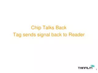
Chip Talks Back Tag sends signal back to Reader. Load Modulation Concepts. I 1. I 2. 2. R1. C1. 1. C2. +. L1. V i. L2. R2. R2 ’. ~. How does I 1 change when switching takes place in secondary (Tag) ?. Let R2’ < R2 When switch moves from position 1 to 2:

E N D
Chip Talks Back Tag sends signal back to Reader
Load Modulation Concepts I1 I2 . . 2 R1 C1 1 C2 + L1 Vi L2 R2 R2’ ~ How does I1 change when switching takes place in secondary (Tag) ? Let R2’ < R2 When switch moves from position 1 to 2: Current in secondary ↑ Current in primary ↓
ISO 14443 Timing Frequency Period Carrier 13.56 MHz 74 ns Sub-carrier =Carrier/16 847 KHz 1.18 ms Bit rate = Sub-carrier/8 105.9 KHz 9.44 ms 9.44 ms ‘1’ - ISO 14443 ‘0’ - ISO 14443 1.18 ms
0 1 Current through Reader Coil Bit duration = 9.44 ms 105.9 Kb/s
Convert to a series resonant circuit I1 I2 C2 . . 2 R1 C1 1 + L1 Vi L2 R2s R2s’ ~ Heuristic Analysis Conditions: Valid at a single frequency Valid for Q >> 1 ≈ XC2/R ≡ C R ≈C Lo to Hi Hi to Lo
Secondary resistance is switching between two values R2s and R2s’ where XC =1/w.C2 for k <<1 Assume both primary and secondary resonant at the excitation frequency w0
Modulation Depth Increases with • Low R1 (High Reader Q) • High R2 (Low tag chip dissipation – High Tag Q) • High k (coupling coefficient) • Higher C2 (Lower L2) (Tag tank capacitance) Above relationship is approximate – need to use with caution Detailed analysis/simulation is often necessary
I1 I2 . . 2 R1 C1 1 C2 + L1 Vi L2 R2 R2’ ~ Approximations If XC2 ~ R2’, then equivalent series capacitance becomes > C2 f02 ↓ and may be < operating frequency • Self-impedance of Tag: Inductive • Transient behavior: slow
More Detailed Analysis (Numerical) Steady StateAnalysis– no transient considerations Modulation Depth: Difference in current in Reader Coil due to switching in Tag - for 1V excitation in Reader Both Reader and Tag tuned to 13.56 MHz L1= 306 nH C1= 450 pF Q1= 8.7 L2= 2755 nH C2 = 50 pF Q2 = 33.5 (unloaded) R2 switched between 5000 and 500 ohms
0.2 0.08 0.02 Effect of Tank Capacitor in Tag
500 ohm 2000 ohm 3000 ohm Effect of Switched Resistance High value of R2: 5000 ohms k = 0.05
Measurement of Load Modulation C1 Tag L1 13.56 MHz Query command C2 Scope ~1 W NFC Forum PD as Reader
0 1 Bit duration = 9.44 ms 105.9 Kb/s
Tag at 5 mm (H = 7.3 A/m) from PD-3 Sub carrier = 13.56/16 MHz = 847.5 KHz ≡ 1.18 ms
Excitation Frequency = 12 MHz Current decreases during switching
Pulse Merge Tag f0 14.0 MHz Tag f0 13.7 MHz
Effect of Tag Resonant Frequency k= 20% 13.56 MHz 13 MHz Good Transient Modulation Index compromised some 14.2 MHz
Trade-off between Q (range) and Bandwidth (data rate) • ISO 14443 : 106 Kb/s, < 10cm • ISO 15693 : 26.5 Kb/s, < 30 cm • Sub-carrier • Higher with higher data rate • ISO 14443 : 847 KHz • ISO 15693 : 484 KHz
Modulation subjected to asymmetric response sc sc sc sc Carrier Carrier +wsc +wsc Carrier Carrier -wsc -wsc Modulation depth is reduced
Load Modulation • Approximate theory • Numerical solution (steady state) • Illustration of simulation • Transients • Measurement • Bandwidth
Parameters Considered • Resonant frequency • Q-factor • Switched resistance • Tank inductor and capacitor
Reader Selected close to 13.56 MHz Tag Sometimes higher than 13.56 MHz Less detuning (choking) effect for multi-tag scenario Pulse merge Resonant frequency
Reader Limited by Bandwidth Close range operation (Blind Spot) Unloaded Q on PCB can be high (~50) but loaded (output resistance of chip) brings loaded Q down. Matching network used Tag Limited by Bandwidth Close range operation (Blind Spot) ESR of tag coil matched to ESR of chip-capacitor combo for maximum power transfer Q factor
Reader NA Tag Modulation depth increases with low R2’ Too low R2’ tends to make Tag inductive during switched state and may degrade transient response Switched Resistance
Reader Large L (low C) helps to increase M (power transfer) Tag Large L (low C) helps to increase M (power transfer) Large C (low L) might help load modulation Less spread in manufacturing (reduced effect from parasitics) 15 to 50 pF is common Tank Inductor, Capacitor
Compensated Antenna Motivation: Stray capacitance creating common mode currents Reduction of effective M Detuning + -V V
C 1 2 C: Common C-1: Compensated Mode – 4 turns C-2: Uncompensated – 8 turns Blue Dot: Via NOT TO SCALE
Tag and Reader Application Requirement of Tag to be attached on or close to metallic surfaces Acting as Reader Or Acting as Tag Antenna could be close to metal
Reader Antenna Automated Inventory with ‘Smart Shelf’ HF system allows more precise location than UHF • HF Reader antenna laid out on metal shelves need spacers • Wasted space • Inconvenience
Eddy (Surface) Currents on Metal Coil B(t) E(t)
Current Carrying Coil near a Metal Sheet ~ Metal Magnetic field has only tangential component over perfect conductor -no normal component Surface (eddy) currents are generated on metal to satisfy above boundary condition
Loop Metal Magnetic Field from a Current Carrying Loop
Performance Degradation • Magnetic field generated by eddy current opposes excitation field • Total flux linked by coil ↓=> Inductance ↓=> Resonant frequency↑ (Mistuning) • Flux linked by secondary loop ↓ => Deterioration in power and signal transfer
Surface Impedance Zs s = conductivity d = skin depth D.F. Sievenpiper, “High Impedance Electromagnetic Surfaces”, Ph.D. Dissertation, University of California, Los Angeles, 1999
Vi = [R1+R0 + j(wL1-1/wC1)].I1 – jwM13.I3 0 = [R3 + jR3].I3 – jwM13.I1 ~ Equivalent Circuit and Phasor Diagram Reader I1 C1 . R1 R0 Metal L1 + . I3 V wL3=R3 F10 45◦ L3 R3 Fresultant F30
Metal B q2 Ferrite m Mitigation with Ferrite Ferrite: High permeability, poor conductivity m0 q1 B0 Bending increases with • mr • thickness I
mr =100 mr =30 Bending Angle
mr.t determines shielding effectiveness • Low cost dielectric spacers help, but need to be much thicker than ferrite for same performance • 0.1 mm ferrite sheet (FK03 – NEC Tokin) allows Tags to be installed on metal surfaces. Dielectric spacers need few cm gap • Loss in ferrite (mr’’) adds additional loss and need to be maintained within limits
Ferrite Image current of source current Image Approach PEC
Antenna Design Issues • Effect of Metal