Startup Transients
Startup Transients. Critical System. Start up Transient - Outputs. FPGA Output. [from Actel Application Note] Power Up

Startup Transients
E N D
Presentation Transcript
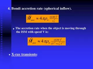
Critical System Start up Transient - Outputs FPGA Output [from Actel Application Note] Power Up Actel FPGAs are nonvolatile and therefore require no external configuration circuitry on power up. However, at power up it does take a finite amount of time for the device to become stable and operate normally. For a VCC slew rate of ~30 ns/V, it takes approximately 250 ms for the device to become fully operational. Power up time varies with temperature, where cold is worst case. At power up, the state of all flip-flops is undefined. Some new designs will be power up safe.
Start up TransientCharge Pump and Isolation Antifuses CHARGE PUMP
Start up Transient - Outputs Fire Cover Arm VCC Hor: 5 ms/Division; Ver: 2 volts/Div
Start up Transient - Inputs FPGA Input During the start up time with many FPGA models, an input may source current. In this application, a buffer with Schmidt trigger inputs is recommended.
Flight Oscillator Start Time 200 kHz +5V 1 ms/div; tRISE = 1 ms
Flight Oscillator Start Time 200 kHz +5V 10 ms/div; tRISE = 50 ms
Synchronous Reset • FPGA may not be functional during power-on transient • Crystal oscillator start time
Startup Current TransientCase Study: RT54SX32 Pre-Irradiation Startup current transient (3.3V supply) of an RT54SX32 pre-irradiation. Voltage at 1V/Div and current at 100mA/Div.
Startup Current TransientCase Study: RT54SX32 Post-Irradiation Startup current transient (3.3V supply) of an RT54SX32 after 98 krad (Si). Voltage at 1V/Div and current at 100 mA/Div.
Startup Current TransientXilinx Technology • Two sets of requirements for the power-on transient for Xilinx XQR4000XL and Virtex 2.5V FPGAs. • Rise time • Current capability of the power supply. • Noted that unlike Actel FPGAs where slower power supply rise times result in higher current values, in Xilinx devices, faster rise times result in higher current values.
Startup Current TransientXilinx XQR4000XL • Rise Time • Slowest power supply rise time is 50 ms. Many power supplies can meet this specification easily • Some spaceborne power supplies may have longer rise times. • Current Levels • The minimum current is broken into two groups: XQR4013-36XL and the XQR4062XL. Note that according to the specification, the values refer to commercial and industrial grade products only, with the transition measured from 0 VDC to 3.6 VDC. Actual currents may be higher than the minimums specified. • Note 3 in the specification states that the duration of the peak current level will be less than 3 ms.
Startup Current TransientXilinx Virtex • Complete power supply requirements are not yet specified in the radiation hard data sheet. Some of the information is taken from the commercial data sheet. • Rise Time • Slowest power supply rise time for this series of parts is 50 ms. • The fastest suggested ramp rate is 2 ms. • May be slow for some power supplies. The parameter measurement criteria on the radiation hard data sheet is from 1 VDC to 2.375 VDC. • Current Levels • The data sheet only specifies a minimum required current supply for Virtex devices at a power supply rise time of 50 ms. • According to the non-military specification, it is 500 mA for commercial grade devices and 2 A for industrial grade parts. • Additionally, shorter power supply rise times will result in higher currents. • The duration of peak currents will be less than 3 ms.
ICC Start-Up Transient Studyin the RT1280A An examination of the effects of radiation, a detailed look at the response of the part, annealing, and impacts to the board-level and system designs.
Figure 1. Startup transient after 4 krad (Si) exposure at 1 krad (Si)/day. The left current peak is unchanged from the pre-irradiation measurement and remained unchanged over the course of this experiment. Analysis on next slide.
Startup transient after 4 krad (Si) exposure at 1 krad (Si)/day. • Left current peak is unchanged from the pre-irradiation measurement and remained unchanged over the course of this experiment. • This current peak is expected as the NMOSFET isolate transistors are not fully conducting, resulting in totem pole currents in the input circuit of the logic modules. • This current level or width is not specified in either the commercial or military specifications. • The 350 mA current peak on the right appears when VCC reaches 3.5 VDC. • The power supply used for these tests had a rise time of < 2 msec. • Voltage is at 1V/div; current is at 100 mA/div.
Figure 2. Startup transient after 5 days of room temperature, biased anneal, following the 4 krad (Si) irradiaton. The radiation-induced current peak is essentially gone. Voltage is at 1V/div; current is at 100 mA/div.
Figure 3. Startup transient after an additional 2 krad (Si) exposure at 1 krad (Si)/day for a total of 6 krads (Si). The radiation-induced current peak is now about 700 mA. Analysis on next slide.
Startup transient after an additional 2 krad (Si) exposure at 1 krad (Si)/day for a total of 6 krads (Si). • The radiation-induced current peak is now about 700 mA. • The current draw still appears when VCC reaches 3.5 VDC, unchanged from the 4 krad (Si) radiation step. • At VCC=3.5VDC, bulk capacitors on the board will have charge Q = 3.5V x C, which will provide charge in addition to that available from the power supply and helping to support the voltage rail. An 18 µF bulk capacitor will store 630 µC. • The current draw for this transient is approximately 100 µC. • Voltage is at 1V/div; current is at 100 mA/div.
Effects of 28-day, biased, room temperature anneal after the 6 krads (Si) irradiation step. • The radiation-induced current peak is now reduced to about 100 mA. • The current draw for this transient is approximately 12 µC, reduced from approximately 100 µC immediately after the 6 krads (Si) exposure. • Voltage is at 1V/div; current is at 100 mA/div.
Figure 5. Effects of 100 °C, biased anneal after the 6 krads (Si) irradiation step and room temperature annealing. The radiation-induced startup current is now virtually eliminated, showing that annealing is effective. Voltage is at 1V/div; current is at 100 mA/div.


