Download
1 / 1
10 likes | 179 Vues
The Train Builder Data Acquisition System for the European-XFEL John Coughlan, Chris Day, Senerath Galagedera and Rob Halsall STFC Rutherford Appleton Laboratory, Oxfordshire, UK E-mail : john.coughlan@stfc.ac.uk. XFEL Data Acquisition

E N D
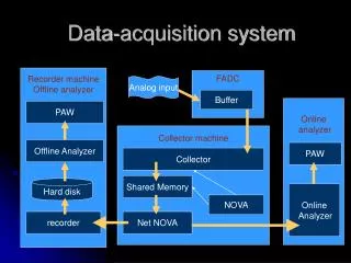
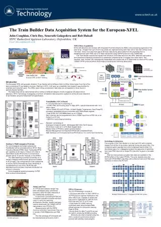
The Train Builder Data Acquisition System for the European-XFEL John Coughlan, Chris Day, Senerath Galagedera and Rob Halsall STFC Rutherford Appleton Laboratory, Oxfordshire, UK E-mail: john.coughlan@stfc.ac.uk XFEL Data Acquisition All the 2D detectors are modular with integrated Front End Electronic (FEE) units processing segments of the pixel array. Images from up to 512 X-ray pulses are captured during each train and a new train arrives every 100 msec. There is an inter-train gap of 99 msec data during which data from the preceding train is transferred from each FEE over a 10 Gbps optical link using UDP/IP protocol to the TrainBuilder. The Train Builder exploits the regular time structure of the data flow from the XFEL detectors and uses a time switched multiplexing architecture to assemble complete series of images from entire trains. The resultant train “movies” are subsequently transmitted over another set of 10 Gbps links to a farm of PCs using 10GbE TCP/IP protocols where final image processing and archiving takes place. Megapixel detector Introduction The European XFEL will generate ultrashort X-ray flashes with a brilliance that is a billion times higher than that of the best conventional X-ray radiation sources. Starting in 2015, it will open up completely new research opportunities for scientists and industrial users. The XFEL beam timing and detector data rates are comparable to those found in particle physics facilities. The beam lines will be instrumented with a number of different designs of multi-megapixel 2D planar silicon detectors. STFC Technology is designing a common off-detector data acquisition system for all the 2D pixel detectors(Train Builder) using the AdvancedTCA specification. European XFEL at DESY Hamburg • TrainBuilder ATCA Board • 4 x I/O channels each comprising of : • VITA57 FMC slot housing dual 10 Gbps SFP+ optical transceivers with 10 G XAUI output. • Xilinx Virtex5 (FX100T) FPGAs. 16 Multi-Gigabit Transceivers. Dual PowerPC processor embedded memory controllers with DMA offload engines. • Dual DDR2 VLP SODIMMs (each up to 2 GByte). • Each channel can be programmed to be a 10GbE Input from a FEE link or an Output to a PC link. • QDRII for local image processing. • Backend comprising of: • Analogue Crosspoint switch (Mindspeed M21145) (72x72 lanes) • ATCA Zone 3 with 32 Tx & Rx Multi-Gigabit lanes. • Master Virtex 5 FPGA for switch synchronisation. • Module Management Unit Spartan3 FPGA with embedded Flash. • GbE interfaces on Front panel and via ATCA Zone 2 for control and monitoring. Switching Architecture The purpose of the Train Builder is to feed each PC with complete images from all the X-ray pulses captured during any given train. The crosspoint switch operates as a time multiplexed barrel shifter. For the simple case of a ¼ Megapixel system the sequence of switching from Input FEE links A-D to Output PC links W-Z is given in the table above. After two train periods complete train data are available in the DDR2 buffers of the output FPGAs. The cycle repeats every two trains with FPGA W&X outputting odd numbered trains and Y&Z even numbers on links to the PC farm. Scaling to Multi-megapixel Systems For one megapixel and larger systems the TrainBuilder will be extended with an ATCA Rear Transition Module (RTM). Each Trainbuilder/RTM pair operates as an Input or Output unit. Data is transmitted via the ATCA Zone 3 connectors to parallel optical Tx and Rx modules on the RTM’s. The data switching is carried out entirely on a central crosspoint switch board (pizza box located in ATCA rack). The configurations of the crosspoints on all the TB ATCA boards are fixed. Switching is coordinated from one of the TB ATCAs with dedicated synchronization channels distributed via a Zone 3 connector. A one megapixel system processing 16 FEE links is shown schematically. Status and Test A n FPGA demonstrator design has been developed using commercial boards to verify the basic elements of the TrainBuilder architecture. A test bench connecting FPGA and Crosspoint evaluation boards has been used to verify the switching architecture. Another system has been used to benchmark the 10GbE UDP/IP transmission from FPGA to PC. Measurements with the DDR2 memory controllers have shown they run in excess of 900 MBytes/sec per FEE link. The first prototype ATCA boards will be manufactured at the end of 2011. • FPGA Firmware • The I/O FPGA design consists of • 10G block with either 10 GbE UDP/IP or TCP/IP protocol engines interfaced to the Xilinx XAUI core. Capable of retries and flow control. Optimised for UDP Rx from FEE links and TCP Tx to PC links. • Dual Power PC DDR2 memory controllers each using multiple DMA offload engines for concurrent memory Read & Write. • Aurora block for data Tx and Rx across the switch, employing 64/66B encoding. • All blocks are interconnectedusing the Xilinx LocalLink synchronous stream protocol with arbitrary frame lengths. Crosspoint switching test bench. Multiple FPGA blocks for ½ megapixel (8 FEE link) system. 10 GbE test bench. 10 G block. Single FPGA blocks.