Download
1 / 48
480 likes | 563 Vues
EECS 373 Design of Microprocessor-Based Systems Mark Brehob University of Michigan Lecture 4 : Bit of ssembly , Memory-mapped I/O, APB January 21, 2014. Today. More assembly review Memory-mapped I/O Bus Architectures ARM AHB-Lite. Example call. main: mov r0, #15 mov r1, #17

E N D
EECS 373 Design of Microprocessor-Based Systems Mark Brehob University of Michigan Lecture 4:Bit of ssembly, Memory-mapped I/O, APB January 21, 2014
Today • More assembly review • Memory-mapped I/O • Bus Architectures • ARM AHB-Lite
Example call main: mov r0, #15 mov r1, #17 blx max loop: b loop min: push {r5} //not needed cmp r0, r1 it gt movgtr1, r0 pop {r5} bxlr • Comments • I’ve left out some directives. • I’ve used an “it” (if-then) block • makes the next instruction conditional • Question • How to change to branch?
Today • More assembly review • Memory-mapped I/O • Bus Architectures • ARM AHB-Lite
Memory-mapped I/O • The idea is really simple • Instead of real memory at a given memory address, have an I/O device respond. • Huh? • Example: • Let’s say we want to have an LED turn on if we write a “1” to memory location 5. • Further, let’s have a button we can read (pushed or unpushed) by reading address 4. • If pushed, it returns a 1. • If not pushed, it returns a 0.
Now… • How do you get that to happen? • We could just say “magic” but that’s not very helpful. • Let’s start by detailing a simple bus and hooking hardware up to it. • We’ll work on a real bus next time!
Basic example • Discuss a basic bus protocol • Asynchronous (no clock) • Initiator and Target • REQ#, ACK#, Data[7:0], ADS[7:0], CMD • CMD=0 is read, CMD=1 is write. • REQ# low means initiator is requesting something. • ACK# low means target has done its job.
A read transaction • Say initiator wants to read location 0x24 • Initiator sets ADS=0x24, CMD=0. • Initiator then sets REQ# to low. (why do we need a delay? How much of a delay?) • Target sees read request. • Target drives data onto data bus. • Target then sets ACK# to low. • Initiator grabs the data from the data bus. • Initiator sets REQ# to high, stops driving ADS and CMD • Target stops driving data, sets ACK# to high terminating the transaction. • Bus is seen to be idle.
0x24 ?? ?? ADS[7:0] CMD Data[7:0] REQ# ACK# 0x55 ?? ?? A B C D E F G HI Read transaction
A write transaction (write 0xF4 to location 0x31) • Initiator sets ADS=0x31, CMD=1, Data=0xF4 • Initiator then sets REQ# to low. • Target sees write request. • Target reads data from data bus. (Just has to store in a register, need not write all the way to memory!) • Target then sets ACK# to low. • Initiator sets REQ# to high & stops driving other lines. • Target sets ACK# to high terminating the transaction
ADS[7] ADS[6] Delay ACK# ADS[5] ADS[4] ADS[3] ADS[2] ADS[1] ADS[0] Data[7] REQ# .. .. .. .. .. 0 Data[0] Button (0 or 1) The push-button(if ADS=0x04 write 0 or 1 depending on button) Button (0 or 1)
ADS[7] ADS[6] Delay ACK# ADS[5] ADS[4] ADS[3] ADS[2] ADS[1] ADS[0] Data[7] REQ# .. .. .. .. .. 0 Data[0] Button (0 or 1) The push-button(if ADS=0x04 write 0 or 1 depending on button) What about CMD?
ADS[7] DATA[7] ADS[6] DATA[6] ADS[5] DATA[5] Delay ACK# ADS[4] DATA[4] D DATA[3] ADS[3] ADS[2] DATA[2] clock ADS[1] DATA[1] Flip-flop which controls LED ADS[0] DATA[0] REQ# The LED(1 bit reg written by LSB of address 0x05)
Let’s write a simple assembly program Light on if button is pressed.
Outline • Finish up example • Bus Architectures • ARM AHB-Lite
What happens when this “instruction” executes? #include <stdio.h> #include <inttypes.h> #define REG_FOO 0x40000140 main () { uint32_t *reg = (uint32_t *)(REG_FOO); *reg += 3; printf(“0x%x\n”, *reg); // Prints out new value }
“*reg += 3” is turned into a ld, add, str sequence • Load instruction • A bus read operation commences • The CPU drives the address “reg” onto the address bus • The CPU indicated a read operation is in process (e.g. R/W#) • Some “handshaking” occurs • The target drives the contents of “reg” onto the data lines • The contents of “reg” is loaded into a CPU register (e.g. r0) • Add instruction • An immediate add (e.g. add r0, #3) adds three to this value • Store instruction • A bus write operation commences • The CPU drives the address “reg” onto the address bus • The CPU indicated a write operation is in process (e.g. R/W#) • Some “handshaking” occurs • The CPU drives the contents of “r0” onto the data lines • The target stores the data value into address “reg”
Details of the bus “handshaking” dependon the particular memory/peripherals involved • SoC memory/peripherals • AMBA AHB/APB • NAND Flash • Open NAND Flash Interface (ONFI) • DDR SDRAM • JEDEC JESD79, JESD79-2F, etc.
Modern embedded systems have multiple busses Atmel SAM3U Expanded 373 focus Historical 373 focus
Advanced Microcontroller Bus Architecture (AMBA)- Advanced High-performance Bus (AHB)- Advanced Peripheral Bus (APB) AHB APB Low power Latched address/control Simple interface Suitable of many peripherals • High performance • Pipelined operation • Burst transfers • Multiple bus masters • Split transactions
Bus terminology • Any given transaction have an “initiator” and “target” • Any device capable of being an initiator is said to be a “bus master” • In many cases there is only one bus master (single master vs. multi-master). • A device that can only be a target is said to be a slave device. • Some wires might be shared among all devices while others might be point-to-point connections (generally connecting the master to each target).
Driving shared wires • It is commonly the case that some shared wires might have more than one potential device that needs to drive them. • For example there might be a shared data bus that is used by the targets and the initiator. We saw this in the simple bus. • In that case, we need a way to allow one device to control the wires while the others “stay out of the way” • Most common solutions are: • using tri-state drivers (so only one device is driving the bus at a time) • using open-collector connections (so if any device drives a 0 there is a 0 on the bus otherwise there is a 1)
Or just say no to shared wires. • Another option is to not share wires that could be driven by more than one device... • This can be really expensive. • Each target device would need its own data bus. • That’s a LOT of wires! • Not doable when connecting chips on a PCB as you are paying for each pin. • Quite doable (though not pretty) inside of a chip.
Wire count • Say you have a single-master bus with 5 other devices connected and a 32-bit data bus. • If we share the data bus using tri-state connections, each device has “only” 32-pins. • If each device that could drive data has it’s own bus… • Each slave would need _____ pins for data • The master would need ______ pins for data • Again, recall pins==$$$$$$.
Outline • Finish up example • Bus Architectures • ARM APB
APB is a fairly simple bus designed to be easy to work with. • Low-cost • Low-power • Low-complexity • Low-bandwidth • Non-pipelined • Ideal for peripherals
Let’s just look at APB writes (Master writing to device)as a starting point. • We’ll add reads shortly.
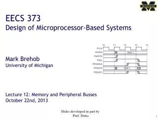
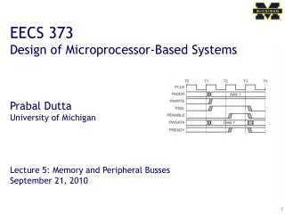
APB bus signals • PCLK • Clock • PADDR • Address on bus • PWRITE • 1=Write, 0=Read • PWDATA • Data written to the I/O device. Supplied by the bus master/processor.
APB bus signals • PSEL • Asserted if the current bus transaction is targeted to this device • PENABLE • High during entire transaction other than the first cycle. • PREADY • Driven by target. Similar to our #ACK. Indicates if the target is ready to do transaction.Each target has it’s own PREADY
Example setup • For the next couple of slides, we will assume we have one bus master “CPU” and two slave devices (D1 and D2) • D1 is mapped to address 0x00001000-0x0000100F • D2 is mapped to 0x00001010-0x0000101F
Say the CPU does a store to location 0x00001004with no stalls D1 D2
32-bit Reg D[31:0] Q[31:0] EN C Design a device which writes to a register wheneverany address in its range is written What if we want to have the LSB of this register control an LED? PWDATA[31:0] PWRITE PENABLE PSEL PADDR[7:0] PCLK PREADY We are assuming APB only gets lowest 8 bits of address here…
32-bit Reg A D[31:0] Q[31:0] EN C 32-bit Reg B D[31:0] Q[31:0] EN C Reg A should be written at address 0x00001000Reg B should be written at address 0x00001004 PWDATA[31:0] PWRITE PENABLE PSEL PADDR[7:0] PCLK PREADY We are assuming APB only gets lowest 8 bits of address here…
Reads… The key thing here is that each slave device has its own read data (PRDATA) bus! Recall that “R” is from the initiator’s viewpoint—the device drives data when read.
Let’s say we want a device that provides data froma switch on a read to any address it is assigned.(so returns a 0 or 1) PRDATA[31:0] PWRITE PENABLE PSEL PADDR[7:0] PCLK PREADY Mr. Switch
Device provides data from switch A if address 0x00001000 is read from. B if address 0x00001004is read from PRDATA[31:0] PWRITE PENABLE PSEL PADDR[7:0] PCLK PREADY Switch A Switch B
32-bit Reg D[31:0] Q[31:0] EN C All reads read from register, all writes write… PWDATA[31:0] PWRITE PENABLE PSEL PADDR[7:0] PCLK PREADY We are assuming APB only gets lowest 8 bits of address here…
Things left out… • There is another signal, PSLVERR (APB Slave Error) which we can drive high if things go bad. • We’ll just tie that to 0. • Notice we are assuming that our device need not stall. • We could stall if we needed. • I can’t find a limit on how long, but I suspect at some point the processor would generate an error.
APB state machine • IDLE • Default APB state • SETUP • When transfer required • PSELx is asserted • Only one cycle • ACCESS • PENABLE is asserted • Addr, write, select, and write data remain stable • Stay if PREADY = L • Goto IDLE if PREADY = H and no more data • Goto SETUP is PREADY = H and more data pending We’ll spend a bit more time on this next week…
Questions? Comments? Discussion?