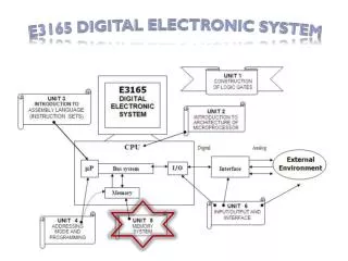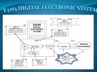
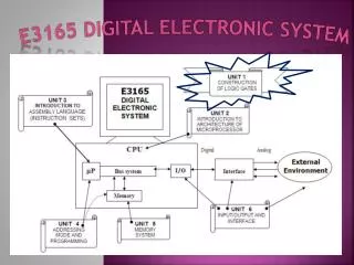
E3165 DIGITAL ELECTRONIC SYSTEM
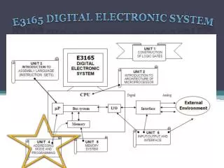
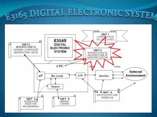
E3165 DIGITAL ELECTRONIC SYSTEM. UNIT 1 – CONSTRUCTION OF LOGIC GATES. 1.0 INTRODUCTION Characteristics of the active electronic components that determine the internal construction and operation of electronic circuitry of a logic gate. UNIT 1 – CONSTRUCTION OF LOGIC GATES.

E3165 DIGITAL ELECTRONIC SYSTEM
E N D
Presentation Transcript
UNIT 1 – CONSTRUCTION OF LOGIC GATES 1.0 INTRODUCTION • Characteristics of the active electronic components that determine the internal construction and operation of electronic circuitry of a logic gate.
UNIT 1 – CONSTRUCTION OF LOGIC GATES 1.1 Types of logic gates • NOT • AND • OR • XOR
UNIT 1 – CONSTRUCTION OF LOGIC GATES 1.1 Types of logic gates (cont.) • NAND • NOR • XOR
UNIT 1 – CONSTRUCTION OF LOGIC GATES 1.2 Diode as a voltage controlled switch • p-n junction component • Two type material: p-type & n-type • Operation: forward biased & reverse biased • Knee voltage: 0.7V (Si) n 0.3V (Ge)
UNIT 1 – CONSTRUCTION OF LOGIC GATES 1.2 Diode as a voltage controlled switch (cont.) • Operation • 0V – knee voltage • Small current’s flow • Beyond knee voltage • Negative voltage • Leakage current • More negative voltage • Zener voltage
UNIT 1 – CONSTRUCTION OF LOGIC GATES 1.2 Diode as a voltage controlled switch (cont.) • Forward biased vs. reverse biased
UNIT 1 – CONSTRUCTION OF LOGIC GATES 1.2 Diode as a voltage controlled switch (cont.) • Diode works as a logic ON/OFF switch
UNIT 1 – CONSTRUCTION OF LOGIC GATES 1.2 Diode as a voltage controlled switch (cont.) • Voltage range of logic level for TTL digital IC
UNIT 1 – CONSTRUCTION OF LOGIC GATES 1.2 Diode as a voltage controlled switch (cont.) • Simple 2-input OR gate
UNIT 1 – CONSTRUCTION OF LOGIC GATES 1.3 Transistor as a voltage controlled switch • p-n junction component • Two type: PNP & NPN
UNIT 1 – CONSTRUCTION OF LOGIC GATES 1.3 Transistor as a voltage controlled switch (cont.) • B-E junction as switch
UNIT 1 – CONSTRUCTION OF LOGIC GATES 1.3 Transistor as a voltage controlled switch (cont.) • Not gate
UNIT 1 – CONSTRUCTION OF LOGIC GATES 1.4 Diode controls switching speed • Speed limitation when switching diode from ON to OFF and vice versa • Minority-carrier density Reverse biased (OFF) Forward biased (ON)
UNIT 1 – CONSTRUCTION OF LOGIC GATES 1.5 Switching time • Rise and fall time • Time taken for a signal to go from LOW to HIGH and vice versa. • Tr and Tf
UNIT 1 – CONSTRUCTION OF LOGIC GATES 1.5 Switching time (cont.) • Storage time (c) Circuit Input waveform Diode current Diode voltage Minority carrier (d) (e)
UNIT 1 – CONSTRUCTION OF LOGIC GATES 1.5 Switching time (cont.) • Propagation delay • Time interval between the application of an input pulse and the occurrence of the resulting output pulse. • Cumulative time delay when gates are cascaded. • Limits the max freq at which a gate can operate. • For propagation delay of 40ns; max freq operation is 25MHz • For propagation delay of 25ns; max freq operation is ???
UNIT 1 – CONSTRUCTION OF LOGIC GATES 1.5 Switching time (cont.) • Propagation delay (cont.) • Two types: • TPLH- delay time from logic 0 to logic 1. • TPHL - delay time from logic 1 to logic 0. • Measured at 50% on rising and falling edges of the input and output. • Total propagation delay?
UNIT 1 – CONSTRUCTION OF LOGIC GATES 1.6 TTL family • TTL Series: • 74 Series – First line of standard TTL ICs • 74L Series – low-power version • 74H Series - high-speed version • 74S Series – Schottky TTL, reduce storage time delay • 74LS Series – Low-Power Schottky TTL • 74AS Series – Advanced Schottky TTL • 74ALS Series – Advanced Low-Power Schottky TTL • 74F Series – Fast TTL
UNIT 1 – CONSTRUCTION OF LOGIC GATES TUGASAN 1 : PETA MINDA. TARIKH AKHIR HANTAR : 12 FEB 2010 1.6 TTL family (cont.) • TTL NAND Gate Operation • Schottky TTL 74S • Low-Power Schottky TTL • Advanced Schottky TTL, 74AS Series (AS-TTL) • Current-Sourcing and Current-Sinking Action • Totem Pole TTL • Tristate (Three-state) TTL NO PLAGIARSM!!!
UNIT 1 – CONSTRUCTION OF LOGIC GATES 1.7 CMOS family • CMOS INVERTER GATE
UNIT 1 – CONSTRUCTION OF LOGIC GATES 1.7 CMOS family • CMOS NAND GATE
UNIT 1 – CONSTRUCTION OF LOGIC GATES 1.7 CMOS family • CMOS TRANSMISSION GATE • Pass signal in both direction. • Useful for digital and analog application.
UNIT 1 – CONSTRUCTION OF LOGIC GATES 1.8 Comparison of CMOS and TTL
UNIT 1 – CONSTRUCTION OF LOGIC GATES 1.9 Interfacing TTL and CMOS ICs • Connecting the output(s) of one circuit of system to the input(s) of another circuit that has different electrical characteristics. • Why? • Utilize strong points of different logic families. • Ex: 74AS used in parts need for highest frequency 741 used in slower parts NMOS for LSI parts of the system. • Two things to consider: • Voltage • Current • Where? – device data sheets
UNIT 1 – CONSTRUCTION OF LOGIC GATES 1.9 Interfacing TTL and CMOS ICs (cont.) • CMOS driving TTL • Input current for CMOS are low compared to output current TTL no prob. • Input voltage for CMOS are higher than output voltage TTL pull-up resistor.