Heterojunctions
Heterojunctions. Two different semiconductor materials that have different energy band gapes are used to form a junction Will introduce a discontinuity at the junction interface Lattice match is important because any lattice mismatch can introduce dislocations resulting in interface states

Heterojunctions
E N D
Presentation Transcript
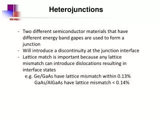
Heterojunctions • Two different semiconductor materials that have different energy band gapes are used to form a junction • Will introduce a discontinuity at the junction interface • Lattice match is important because any lattice mismatch can introduce dislocations resulting in interface states • e.g. Ge/GaAs have lattice mismatch within 0.13% • GaAs/AlGaAs have lattice mismatch < 0.14%
Energy-band diagram • We consider only the case of “straddling” here • Those in which he dopant type changes at the junction are called isotype • e.g. n-P, N-p • Those in which he dopant type is the same at the junction are called anisotype • e.g. n-N, p-P
Energy-band diagram - Flow of charges creates a space charge region in the vicinity of the metallurgical junction
Two-Dimensional Electron Gas • Energy band diagram of n-N GaAs-AlGaAs • AlGaAs can be moderately doped or heavily doped, GaAs can be lightly doped or intrinsic • Electron flow forms an accumulation layer of electrons in the potential well adjacent to the interface • 2-D electron gas refers to the condition in which electrons have quantized energy levels perpendicular to the interface, but are free to move in the other two spatial directions
Conduction band edge and potential well • Quantized energy levels • Current parallel to the interface will be a function of the electron concentration shown on the figure and of the mobility
Graded heterojunction • 2-D electron gas is in a region of low impurity doping so that impurity scattering effects are minimized, • electron mobility will be much higher than if electrons • were in the same region as the ionized donors • Movement of electrons papallel to the interface will still influenced by • coulomb attraction of ionized impurities in AlGaAs • Graded layer resolve the problem