Download
1 / 12
160 likes | 398 Vues
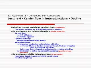
6.772/SMA5111 - Compound Semiconductors Lecture 4 - Carrier flow in heterojunctions - Outline . • A look at current models for m-s junctions (old business) Thermionic emission vs. drift-diffusion vs. p-n junction • Conduction normal to heterojunctions (current across HJs)

E N D
6.772/SMA5111 - Compound SemiconductorsLecture 4 - Carrier flow in heterojunctions - Outline • A look at current models for m-s junctions(old business) Thermionic emission vs. drift-diffusion vs. p-n junction • Conduction normal to heterojunctions(current across HJs) Current flow: 1. Drift-diffusion 2. Ballistic injection Injection tailoring: decoupling injection from doping Band-edge spikes: 1. Impact on conduction and evolution with bias: a. Forward flow: i. Barriers to carrier flow; ii. Division of applied bias; iii. Evolution with bias b. Reverse flow: i. impact on collection; ii. evolution with bias 2. Elimination of spikes by composition grading (quasi-Fermi level discussion) • Conduction parallel to heterojunctions (in-plane action) Modulation doped structures:Mobility vs. structure Interface roughness
Applying bias to a metal-semiconductor junction, review • Currents Note: the barrier seen by electrons in the metal does not change with bias, whereas the barrier seen by those in the semiconductor does. Thus the carrier flux (current) we focus on is that of majority carriers from the semiconductor flowing into the metal. Metal-semiconductor junctions are primarily majority carrier devices. (Minority carrier injection into the semiconductor can usually be neglected; more about this later)
M-S JUNCTION CURRENT MODELS: General form of net barrier current: comparing models id= A q R ND e [-qΦb/ kT]( e [qvAB/ kT]-1) Thermionic emission model - ballistic injection over barrier id /A= A*T[2]d / A = ( e [qvAB/ kT]-1) A*: Thermionic emission coefficient Φbm: Barrier in metal, =Φb + (kT /q) ln(NC/ ND) Substituting for Φbm and rearranging : id /A=q(A*T[2]/qNC) ND e [-qΦb/ kT]( e [qvAB/ kT]-1) from which we see RTE = A*T[2]/qNC
Drift-diffusion model - drift to and over barrier id/A= qμe EpkND e [-qΦb/ kT]( e [qvAB/ kT]-1) Where : Epk: Peak electric field, =E(0) =√ 2q(Φb-vAB)ND/ε Comparing this to the stan dard form we see : RDD =μe Epk,which is the drift velocity at x =0! Before comparing the thermionic emission and drift-diffusion expressions, we will look at the current through a p-n+ junction diode.
Comparing the results Thermionic emission RTE= A*T2/qNC, modeling from metal side RTE Drift-diffusion RDD =μe Epk , the drift velocity at x =0. p-n+ diode R p-n += De / wp , the diffusion velocity.
Conduction normal to heterojunctions Emitter efficiency expressions with and without spike, and comparison with homojunction result Grading composition to eliminate spikes: WHITE BOARD Quasi-Fermi levels and built-in effective fields due to band-edge slopes ∂Ec/∂x for electrons, ∂Ev/∂x for holes
Homojunctions - band picture, depletion approximation • Electrically connected: i. Charge shifts between sides ii. Fermi levels shift until equal iii. Vacuum ref. is now -qf(x) where f(x) = (q/e)∫∫r(x) dx dx iv. Ec(x) is -qf(x) -c(x) and Ev(x) = -qf(x) - [c(x) +Eg(x)] v. Depletion approximation is a
Conduction parallel to heterojunctions Modulation doped structures N-n heterojunctions and accumulated electrons Modulation doped structure with surface pinning and HJ WHITE BOARD Back to foils Carrier scattering and mobilities in accumulated two-dimensional electron gas
Modulation doping - two-dimensional electron gases • Components of mobility GaAs (Image deleted) See Fig 1-9-2 in: Shur, M.S. Physics of Semiconductor Devices Englewood Cliffs, N.J., Prentice-Hall, 1990.
Modulation doping - two-dimensional electron gases • Bulk mobilities in GaAs as a function of doping level (at room temperature) (Image deleted) See Ch2 Fig19 in: Sze, S.M. Physics of Semiconductor Device 2nd ed. New York: Wiley, 1981.
Modulation doping - two-dimensional electron gases • Improvement of TEG mobility with time (Image deleted) See Fig 60 in: Weisbuch, C. and Vinter, B., Quantum Semiconductor Structures: Fundamentals and Applications Boston: Academic Press, 1991.