Download
1 / 3
30 likes | 420 Vues
Microwave and Wireless Engineering Program. Bradley University . Distributed Power Amplifiers-Output Power and Efficiency Considerations. Prasad N. Shastry (S. N. Prasad) 1 , Senior Member, IEEE, and Amir S. Ibrahim 2.

E N D
Microwave and Wireless Engineering Program Bradley University Distributed Power Amplifiers-Output Power and Efficiency Considerations Prasad N. Shastry (S. N. Prasad)1 , Senior Member, IEEE, and Amir S. Ibrahim2 1Department of Electrical and Computer Engineering, Bradley University, Peoria, IL, 2Mobile Devices, Motorola Inc., Libertyville, IL
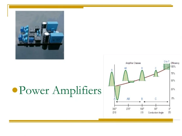
Microwave and Wireless Engineering Program Bradley University Abstract In this paper the efficiency and output power limitations of distributed amplifiers (DAs) and techniques to overcome the limitations are addressed, and the analysis, design, and measured results of a tapered drain line distributed power amplifier are presented in detail for the first time. The DA has a gain of 10 dB, power-added-efficiency of 24%, and output power of about 20 dBm, over a 4.5 GHz bandwidth. Further, the efficiency of the tapered drain line DA is shown to be comparable to a reactively matched power amplifier using the same number and type of transistors. The topology of the tapered drain line DA is suitable for monolithic implementation. Gain Comparison Between DAs, Reactively Matched Amplifiers, and Tapered Drain Line DAs • Power and efficiency limiting factors in a distributed amplifier • Transistor pinch-off • Unequal contribution by transistors to output power • Transistor gate-drain breakdown • Un-utilized power in the reverse wave • Non-optimum load impedance presented to transistors • Tapered drain line distributed amplifier • Each transistor must see its optimal load impedance, ROPT. • Drain line consists of line segments of varying characteristic impedance connected between the output terminals of the cells. • The characteristic impedance of the line segment between cells “m” and “m+1” is given by, Zom = ROPT/m. • Gate line is designed as in a conventional lowpass distributed amplifier. • Simulation Results and Analysis • Transistor : NE721; Number of transistors : 4; Frequency range: 0-4.5 GHz; DC-Bias for each transistor: Vds = 3V; Vgs = -0.675V; Ids = 30 mA. • Conventional lowpass distributed amplifier: • Image impedance of gate and drain lines: 50 Ω. • Reactively matched balanced amplifier: • Optimum load and source impedances at 2 GHz: ZL = 56.32 + j14.43 Ω; ZS = 62.02 + j59.67 Ω • Tapered drain line distributed amplifier: • Optimum load impedance (ROPT) presented to each transistor: 50 Ω • Image impedance of gate line : 50 Ω • Wideband output matching network-to convert 50 Ω to 12.5 Ω (ROPT/4) • Delays on the drain line equal the delays on the gate line. • No termination on the drain line. Tapered drain line, conventional gate line-distributed power amplifier. PAE (%) Comparison Between DAs, Reactively Matched Amplifiers, and Tapered Drain Line DAs P1dB Comparison Between DAs, Reactively Matched Amplifiers, and Tapered Drain Line DAs Logical construction of the drain line of the tapered drain line of a distributed amplifier. http://cegt201.bradley.edu/rfpage
Microwave and Wireless Engineering Program Bradley University • Transistor: NE 721 ; Number of transistors: 4 • Amplifier DC-Bias: Vds = 3V; Vgs = -0.74V; Ids (total) = 120 mA • Circuit Boards: • Gate line : εr = 3.1; h = 30 mil • Drain line: εr = 10 ; h = 25 mil • Heat Sink material: Brass Picture of the amplifier (including the heat sink) Conventional Distributed amplifier Conclusions A tapered drain line DA having a gain of 10dB and power-added efficiency of 24% over a 4.5 GHz band has been realized. The results showed that the tapered drain line approach increased the power-added-efficiency from about 11% to 24% across the 4.5 GHz band. This relatively high value of efficiency for a DA is comparable to the 27% power-added-efficiency of the reactively matched power amplifier. Acknowledgment The authors would like to thank Mr. Balamurugan Sundaram and Mr. Sureshbabu Sundaram, graduate students, Department of Electrical and Computer Engineering, Bradley University, for preparing the illustrations and formatting this paper. Plot showing simulated and measured magnitudes of S21. A four-stage balanced power amplifier. Measured gain compression at three different frequencies. Distribution of power on the drain line for a tapered drain line DA Layout of the amplifier with output matching network Measured third and fifth order intermodulation levels versus input power. http://cegt201.bradley.edu/rfpage