Power Amplifiers
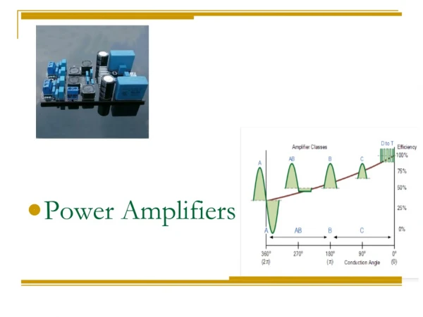
Power Amplifiers. Unit – 4.1. Classification of Power Amplifiers. Power amplifiers are classified based on the Q point If the operating point is chosen at the middle of the load line, it is called Class A amplifier

Power Amplifiers
E N D
Presentation Transcript
Power Amplifiers Unit – 4.1
Classification of Power Amplifiers • Power amplifiers are classified based on the Q point • If the operating point is chosen at the middle of the load line, it is called Class A amplifier • If the operating point is chosen at the cut-off point it is called Class B amplifier • If the operating point is chosen beyond the cut-off point it is called Class C amplifier • It conducts for 3600
Class A amplifier • The Q point is chosen at the middle of load line • This will give equal swing on either direction • Both halves of the input comes at the output • Hence Class A will give (amplitude) distortionless output • It can handle only small signals • Its efficiency is less
10mA Ic B 6mA Ib = 60μA 10mA 4mA Ib = 50μA 8mA Q Ib = 40μA 6mA Ib = 30μA 4mA Ib = 20μA 2mA A Vce 0 V 24 V Class A
Class B amplifier • The Q point is chosen at the cut-offpoint • This will give swing only on one direction • Only one half of the input comes at the output • Hence Class B will give (amplitude) distorted output • It can handle large signals • Its efficiency is high • It conducts for 1800
10mA Ic Ib = 60μA 10mA Ib = 50μA 8mA Ib = 40μA 6mA Ib = 30μA 0mA 4mA Ib = 20μA 2mA Q Vce 0 V 24 V Class B
Class C amplifier • The Q point is chosen at the beyond the cut-offpoint • This will give only a partial swing in one direction • Only a portion of the input comes at the output • Hence Class C will give (amplitude) severely distorted output • It can handle large signals • It conducts for less than 1800
10mA Ic Ib = 60μA 10mA Ib = 50μA 8mA Ib = 40μA 6mA Ib = 30μA 0mA 4mA Ib = 20μA 2mA Q` Vce 0 V 24 V Class C
Class A Class B Class C
Distortionless amplifier • Out of the 3 amplifiers, Class C is unsuitable as the distortion is very heavy • Class A is the best, as it gives distortionless output • But Class A cannot handle large signals as required by the Power Amplifier • Though Class B gives heavy distortion, it gives out one half of the signal perfectly • And Class B can handle large signals
Class A Audio Amplifier • As we have seen out of the 3 classifications, Class A is the best, as it does not give any distortion • Among the configurations, we know that CE is the best as it gives maximum power gain • A CE amplifier will have high output impedance • Unfortunately for an audio amplifier, the output device is the speaker which has a low impedance
Impedance Matching • The speaker impedance is typically about 4 Ω • Hence there is a mismatch between the high Zo of the amplifier and the low impedance of the speaker • This will result in loss of gain • This can be avoided by connecting a transformer at the output stage • The primary winding will match the high Zo of the amplifier while the secondary will match the low impedance of the speaker
Class A Audio Amplifier Vcc Rb1 Rb1 Rc 270 K 5.6 K 270 K Rb2 Re Rb2 Re Ce Ce
Drawback • The drawback of this circuit is that it cannot handle large signals • In a Class A amplifier, the operating point is chosen around the middle of the load line • If the signal exceeds the cut-off point, the output current stops and any signal with a lower amplitude will not come at the output • Similarly, if the signal exceeds the saturation point, the output current cannot increase any further, even if the input signal increases
Class A Ic B Ib = 60μA 10mA Ib = 50μA 8mA Q Ib = 40μA 6mA Ib = 30μA 4mA Ib = 20μA 2mA A Vce 0 V 24 V
Class B Push-Pull Amplifier • To avoid this we can use Class B which has a greater signal handlingcapacity • But Class B will give only one half of the signal • Hence we can use 2 Class B amplifiers • One for one half and one for the other half • This type of amplifier is called Push-Pull Amplifier
Vcc T1 TR1 TR2 T3 T2 Class B Push-Pull
Push-Pull Circuit • TR1 and TR2 are output transistors connected back to back, with their emitters grounded • The output transformerTR1 couples the push-pull output to the speaker • In the Push-Pull arrangement T1 conducts for one half of the signal & T2 conducts for the other half • Both are biased in Class B and each gives one half of the signal & the combined output is coupled to the speaker
Push-Pull Circuit • The Driver TransformerTR2 gives 2 out of phase signals • During one half, the +ve half forward biases T1 while the –ve half reverse biases T2 • Thus when T1 conducts, T2 is cut-off & vice-versa • This way both the transistors conduct alternately to give the full signal output
Class D Amplifier • During the +ve half cycle Q1 gets Forward Bias and it conducts • During the -ve half cycle Q2 gets Forward Bias and it conducts • Thus both the transistors conduct alternately • The amplifier works for 3600 • No distortion • 100% efficiency
Vcc T1 TR1 TR2 T3 T2 Working of Push-Pull Circuit • During the first half T1 conducts • Ic flows from the centre-tapping through T1 to ground • This half is coupled to the speaker through TR1
Vcc T1 TR1 TR2 T3 T2 Working of Push-Pull Circuit • During the second half T2 conducts • Ic flows from the centre-tapping through T2 to ground • This half is coupled to the speaker through TR1
Drawbacks • Though this circuit functions well it has a few drawbacks • Transformer coupling affects the quality of output • Phase shifting circuit is a must • Both these drawbacks can be avoided if we use one pair of PNP and NPN transistors at the output
Complementary Symmetry Amplifier Vcc T1 T2
Complementary Symmetry Amplifier • This circuit uses one NPN transistor & one PNP transistor at the output stage • During the +ve half, T1(NPN) base gets forward bias & it conducts while T2 (PNP) gets reverse biased and does not conduct • This gives one half of the signal at the speaker coupled to the emitter
Complementary Symmetry Amplifier • During the other half, T2 gets forward bias and conducts while T1 gets reverse biased and does not conduct • Thus T1 & T2 conduct alternately giving a distortionless output • This circuit does not require a phase shifter
Cross – over distortion • Class B Push-Pull amplifier has one limitation • As the phase of the signal changes from +ve to –ve (or vice-versa) one transistor stops conducting while the other begins conducting • But the transistor cannot conduct instantaneously as it requires a minimum Vbe before it starts conducting • Thus as the signal crosses over zero, a distortion occurs • This is called Cross over distortion
Cross – over distortion Vbe -Vbe
Class AB amplifier • This circuit overcomes cross-over distortion • Biasing is done such that even if there is no input signal, a small current keeps the output transistor conducting • This circuit uses 2 diodes whose characteristics matches with that of the BE junction of the output transistors • Biasing resistors R1 & R2 are also identical values
Class AB amplifier Vcc R1 T1 D1 D2 T2 R2
Symmetrical components • Since R1 & D1 are identical to R2 & D2, the diode junction as well as the output point will be at half the supply voltage • Because of symmetry both T1 & T2 will conduct equally • Even when there is no input signal, there will be a current Icq = (I/2 Vcc – 0.6) / R1 • This will keep the output transistors conducting
Elimination of cross-over distortion • Normally, during cross-over there will not be any output till the non-conducting transistor gets the minimum Vbe • This causes distortion • This has been eliminated here, since the 0.6 V across the diodes keep the transistors on and gives a continuous output signal without producing cross-over distortion
Thermal stability • In addition, the two diodes also provide thermal stability • They prevent the output transistors going to Thermal Run Away • When the output current is high, heat dissipation is more • The increase in temperature produces more charge carrier in the BE junction of T1 & T2
This increases Ib & hence Ic • This in turn increases the power dissipation & hence the heat • This chain goes on till too much current flows and destroys the transistors • This is called Thermal Run Away • This is arrested by the diodes in the output circuit
When the charge carriers increase in the B-E junction of T1 & T2, a similar increase takes place in D1 & D2, due to matching characteristics • This increase in the diode current, produces more drop across R1 & R2 and brings down the forward bias at the base of T1 & T2 • Thus the 2 diodes prevent cross-over distortion as well as provide thermal stability