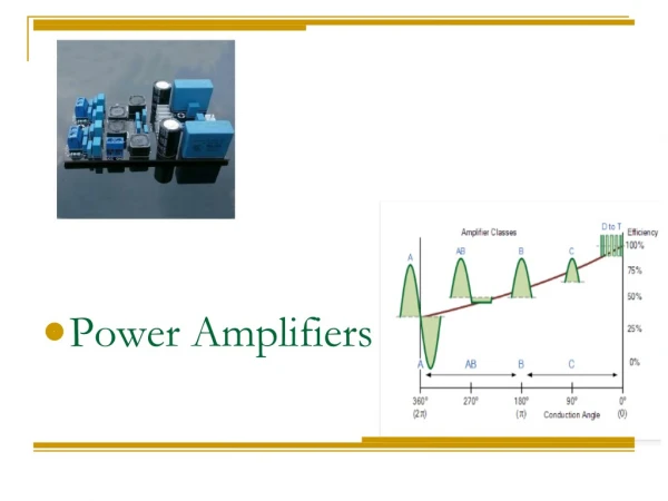
Chapter 12 Power Amplifiers
Chapter 12 Power Amplifiers. 12.1 General Considerations 12.2 Classification of Power Amplifiers 12.3 High-Efficiency Power Amplifiers 12.4 Cascode Output Stages 12.5 Large-Signal Impedance Matching 12.6 Basic Linearization Techniques 12.7 Polar Modulation 12.8 Outphasing

Chapter 12 Power Amplifiers
E N D
Presentation Transcript
Chapter 12 Power Amplifiers • 12.1 General Considerations • 12.2 Classification of Power Amplifiers • 12.3 High-Efficiency Power Amplifiers • 12.4 Cascode Output Stages • 12.5 Large-Signal Impedance Matching • 12.6 Basic Linearization Techniques • 12.7 Polar Modulation • 12.8 Outphasing • 12.9 Doherty Power Amplifier • 12.10 Design Examples Behzad Razavi, RF Microelectronics. Prepared by Bo Wen, UCLA
Chapter Outline • Class A PAs • Class B PAs • Class C PAs • Class A PAs with Harmonic Enhancement • Class E PAs • Class F PAs PA Design Examples Linearization Techniques High Efficiency PAs Basic PA Classes • Feedforward • Cartesian Feedback • Predistortion • Polar Modulation • Outphasing • Doherty PA • Cascode PAs • Positive-Feedback PAs • PAs with Power Combining • Polar Modulation PAs • Outphasing PAs
The Trade-Off between the Output Power and the Voltage Swing • For a common-source (or common-emitter) stage to drive the load directly, a supply voltage greater than Vpp is required. • If the load is realized as an inductor, the drain ac voltage exceeds VDD, even reaching 2VDD (or higher). But the maximum drain-source voltage experienced by M1 is still at least 20 V if the stage must deliver 1 W to a 50-Ω load. • It can be proven that the product of the breakdown voltage and fT of silicon devices is around 200 GHz·V.
Example of RF Choke What is the peak current carried by M1 in figure below? Assume L1 is large enough to act as an ac open circuit at the frequency of interest, in which case it is called an “RF choke” (RFC). Solution: If L1 is large, it carries a constant current, IL1 (why?). If M1 begins to turn off, this current flows through RL, creating a positive peak voltage of IL1RL. Conversely, if M1 turns on completely, it must “sink” both the inductor current and a negative current of IL1 from RL so as to create a peak voltage of -IL1RL. The peak current through the output transistor is therefore equal to 400 mA.
Interposing a Matching Network • In order to reduce the peak voltage experienced by the output transistor, a “matching network” is interposed between the PA and the load. This network transforms the load resistance to a lower value, RT , so that smaller voltage swings still deliver the required power. The above PA must deliver 1 W to RL = 50 Ω with a supply voltage of 1 V. Estimate the value of RT. The peak-to-peak voltage swing, Vpp, at the drain of M1 is approximately equal to 2 V. Since: The matching network must therefore transform RL down by a factor of 100. Figure above shows an example, where a lossless transformer having a turns ratio of 1:10 converts a 2-Vpp swing at the drain of M1 to a 20-Vpp swing across RL.
Example of Inductive-Loaded CS Stage Plot VX and Vout in figure below as a function of time if M1 draws enough current to bring VX near zero. Assume sinusoidal waveforms. Also, assume L1 and C1 are ideal and very large. Solution: In the absence of a signal, VX = VDD and Vout = 0. Thus, the voltage across C1 is equal to VDD. We also observe that, in the steady state, the average value of VX must be equal to VDD because L1 is ideal and therefore must sustain a zero average voltage. That is, if VX goes from VDD to near zero, it must also go from VDD to about 2VDD so that the average value of VX is equal to VDD . The output voltage waveform is simply equal to VX shifted down by VDD.
Effect of High Currents • If the output transistor is chosen wide enough to carry a large current, then its input capacitance is very large, making the design of the preceding stage difficult. • We may deal with this issue by interposing a number of tapered stages between the upconversion mixer(s) and the output stage. • Another issue arising from the high ac currents in PAs relates to the package parasitic. • The large currents can also lead to a high loss in the matching network.
Example of Package Parasitics The output transistor in previous example with a transformer carries a current varying between 0 and 4 A at a frequency of 1 GHz. What is the maximum tolerable bond wire inductance in series with the source of the transistor if the voltage drop across this inductance must remain below 100 mV? Solution: The drain current of M1 can be approximated as where I0 = 2 A and ω0 = 2π(1 GHz). The voltage drop across the source inductance, LS, is given by reaching a peak of LSω0I0. For this drop to remain below 100 mV, we have This is an extremely small inductance.(A single bond wire’s inductance typically exceeds 1 nH)
Efficiency The “drain efficiency” (for FET implementations) or “collector efficiency” (for bipolar implementations) is defined as: where PL denotes the average power delivered to the load and Psupp the average power drawn from the supply voltage. “Power-added efficiency”, PAE, defined as where Pin is the average input power Discuss the PAE of the CS stage. At low to moderate frequencies, the input impedance is capacitive and hence the average input power is zero. (Of course, driving a large capacitance is still difficult.) Thus, PAE = η. At high frequencies, the feedback due to the gate-drain capacitance introduces a real part in Zin, causing the input port to draw some power. Consequently, PAE < η. In stand-alone PAs, we may deliberately introduce a 50-Ω input resistance, in which case PAE < η.
Linearity: PA Characterization • The PA characterization begins with two generic tests of nonlinearity based on unmodulated tones: intermodulation and compression. A more rigorous characterization: suppose the modulated input is of the form: The output can be written as: Assume both A(t) and Φ(t) are nonlinear static functions of only the input amplitude, a(t)
AM/AM Conversion and AM/PM Conversion and Rapp Model A[a(t)] and Φ[a(t)] represent “AM/AM conversion” and “AM/PM conversion”, respectively • For a cascade of stages, the overall model may be quite complex and the behavior of A and Φ quite different. Another PA nonlinearity representation, called the “Rapp model”, is expressed as follows: • Dealing with only static nonlinearity, this model has become popular in integrated PA design. We return to it in Chapter 13.
Single Ended PAs (Ⅰ) • Advantages of single ended PAs: the antenna is typically single-ended, and single-ended RF circuits are much simpler to test than their differential counterparts. • Drawback No.1: they “waste” half of the transmitter voltage gain because they sense only one output of the upconverter. • This issue can be alleviated by interposing a balun between the upconverter and the PA. But balun introduces its own loss.
Single Ended PAs (Ⅱ) • Drawback No.2 stems from the very large transient currents that they pull from the supply to the ground. • LB1 alters the resonance or impedance transformation properties of the output network if it is comparable with LD. LB1 allow some of the output stage signal to travel back to the preceding stages. LB2 degenerates the output stage and introduces feedback.
Differential PAs • A differential realization draws much smaller transient currents from VDD and ground lines, exhibiting less sensitivity to LB1 and LB2 and creating less feedback. The degeneration issue is also relaxed considerably. • While the use of a differential PA ameliorates both the voltage gain and package parasitic issues, the PA must still drive a single-ended antenna in most cases. Thus, a balun must now be inserted between the PA and the antenna.
Example of Efficiency and Loss in Balun Design Suppose a given balun design has a loss of 1.5 dB. In which one of the transmitters shown before (one with balun preceding PA and one after PA)does this loss affect the efficiency more adversely? Solution: In the former case, the balun lowers the voltage gain by 1.5 dB but does not consume much power. For example, if the power delivered by the upconverter to the PA is around 0 dBm, then a balun loss of 1.5 dB translates to a heat dissipation of 0.3 mW. In the latter one, on the other hand, the balun experiences the entire power delivered by the PA to the load, dissipating substantial power. For example, if the PA output reaches 1 W, then a balun loss of 1.5 dB corresponds to 300 mW. The TX efficiency therefore degrades more significantly in the latter case.
Classification of Power Amplifiers: Class A Power Amplifiers • Class A amplifiers are defined as circuits in which the transistor(s) remain on and operate linearly across the full input and output range. • If linearity is required, then class A operation is necessary. The maximum drain efficiency of class A amplifiers:
Examples of Class A Power Amplifiers Is the foregoing calculation of efficiency consistent with the assumption of linearity in class A stages? No, it is not. With a sinusoidal input, VX reaches 2VDD only if the transistor turns off. This ensures that the current swing delivered to the load goes from zero to twice the bias value. Explain why low-gain output stages suffer from a more severe efficiency-linearity trade-off. Consider the two scenarios depicted in figure below. In both cases, for M1 to remain in saturation at t = t1, the drain voltage must exceed V0 + Vp,in - VTH. In the high-gain stage, Vp,in is small, allowing VX to come closer to zero than in the low-gain stage.
Efficiency in Different Scaling Scenarios (1)The supply voltage and bias current remain at the levels necessary for full output power and only the input signal swing is reduced: (2)The supply voltage remains unchanged but the bias current is reduced in proportion to the output voltage swing: (3)Both the supply voltage and the bias current are reduced in proportion to the output voltage swing:
Example of Output Stage with Variable Supply Voltage A student attempts to construct an output stage with a variable supply voltage as shown below. Here, M2 operates in the triode region, acting as a voltage-controlled resistor, and C2 establishes an ac ground at node Y . Can this circuit achieve an efficiency of 50%? Solution: No, it cannot. Unfortunately, M2 itself consumes power. If the bias current is chosen equal to Vp=Rin, then the total power drawn from VDD is still given by (Vp/Rin)VDD regardless of the on-resistance of M2. Thus,M2 consumes a power of (Vp/Rin)Ron2, where Ron2 denotes its on-resistance.
Class B Power Amplifier • Conduction Angle is defined as the percentage of the signal period during which the transistor remain on multiplied by 360 ° • The traditional class B PA employs two parallel stages each of which conducts for only 180°, thereby achieving a higher efficiency than the class A counterpart.
Example of Class B Amplifier Explain how T1 combines the half-cycle current waveforms generated by M1 and M2 Solution: Using superposition, we draw the output network in the two half cycles as shown here. When M1 is on, ID1 flows from node X, producing a current in the secondary that flows into RL and generates a positive Vout . Conversely, when M2is on and draws current from node Y , the secondary current flows out of RL and generates a negative Vout
Issue of Output Swing of Class B PA/ Class AB PA • If the parasitic capacitances are small and the primary and secondary inductances are large, the swing above VDD is approximately half that below VDD, an undesirable situation resulting in a low efficiency. • For this reason, the secondary (or primary) of the transformer is tuned by a parallel capacitance. • The term “class AB” is sometimes used to refer to a single-ended PA (e.g., a CS stage) whose conduction angle falls between 180 ° and 360 °, i.e., in which the output transistor turns off for less than half of a period. From another perspective, a class AB PA is less linear than a class A stage and more linear than a class B stage.
Calculation of Class B PA Efficiency(Ⅰ) A half-cycle sinusoidal current, ID1 = Ipsinω0t, producing an output voltage given by: and delivering an average power of: average power provided by VDD is equal to: Drain efficiency of class B stages:
Calculation of Class B PA Efficiency(Ⅱ) In our last step, we calculate the voltage swings at X and Y in the presence of a resonant load in the secondary (or primary). The primary of the transformer therefore senses a voltage waveform given by which, upon experiencing a ratio of n/(2m), yields the output voltage: We choose Vp = VDDto maximize the efficiency
Class C Power Amplifiers: Overview • In class C stages, the conduction angle is further reduced. In order to avoid large harmonic levels at the antenna, the matching network must provide some filtering. • As θ decreases, the transistor is on for a smaller fraction of the period, thus dissipating less power. For the same reason, however, the transistor delivers less power to the load.
Efficiency of Class C Power Amplifiers • Efficiency of 100% as θapproaches zero. • Pout falls to zero as θ approaches zero.
Example of Class C Stage Harmonic Calculation Determine the amplitude of the first harmonic of the transistor drain current Class C stage for a conduction angle of θ. Consider the waveform shown here, where conduction begins at point A and ends at point B. The angle of the sinusoid reaches α at A and π-α at B such that π-α-α= θand hence α = (π-θ)/2. The Fourier coefficients of the first harmonic are obtained as hence the first harmonic is expressed as Note that a1 → 0 as α → π/2. For example, if α = π/4, then a1 ≈ 0:41Ip, the transistor must therefore be about 2.4 times as large as in a class-A stage for the same output power. Upon multiplication by Rin, this harmonic must yield a drain voltage swing of nearly 2VDD.
High-Efficiency Power Amplifiers: Class A Stage with Harmonic Enhancement • Suppose the matching network is designed such that its input impedance is low at the fundamental and high at the second harmonic. • The average power consumed by the output transistor decreases and the efficiency increases.
Class E Stage: Revisiting Output Stage with Switching Transistor • Class E stages are nonlinear amplifiers that achieve efficiencies approaching 100% while delivering full power, a remarkable advantage over class C circuits. • Called a “switching power amplifier,” such a topology achieves a high efficiency if : • (1) M1 sustains a small voltage when it carries current, • (2) M1 carries a small current when it sustains a finite voltage • (3) the transition times between the on and off states are minimized
Dealing with Finite Input and Output Transitions • The gate of the output device must be switched as abruptly as possible to maximize the efficiency, but the large output transistor typically necessitates resonance at its gate, inevitably receiving a nearly sinusoidal waveform. • Class E amplifiers deal with the finite input and output transition times by proper load design.
Three Conditions Required for Vx • (1) As the switch turns off VX remains low long enough for the current to drop to zero, i.e., VX and ID1 have nonoverlapping waveforms. The first condition resolves the issue of finite fall time at the gate of M1. • (2)Vxreaches zero just before the switch turns on. The second condition ensures that the VDS and ID of the switching device do not overlap in the vicinity of the turn-on point, thus minimizing the power loss. • (3)dVx /dt is also near zero when the switch turns on. The third condition lowers the sensitivity of the efficiency to violations of the second condition. • The time response depends on the Q of the network and appears as shown above for underdamped, overdamped and critically-damped conditions.
Example of Class E Stage (Ⅰ) Modeling a class E stage as shown below, plot the circuit’s voltages and currents When M1 turns on, it shorts node X to ground but carries little current because VX is already near zero at this time (second condition described above). If Ron1 is small, VX remains near zero and LD sustains a relatively constant voltage, thus carrying a current given by
Example of Class E Stage (Ⅱ) Modeling a class E stage as shown below, plot the circuit’s voltages and currents In other words, one half cycle is dedicated to charging LD with minimal drop across M1. When M1 turns off, the inductor current begins to flow through C1 and the load, raising VX. This voltage reaches a peak at t = t1and begins to fall thereafter, approaching zero with a zero slope at the end of the second half cycle (second and third conditions described above). The matching network attenuates higher harmonics of VX, yielding a nearly sinusoidal output.
Class F Power Amplifiers • If in the generic switching stage the load network provides a high termination impedance at the second or third harmonics, the voltage waveform across the switch exhibits sharper edges than a sinusoid, thereby reducing the power loss in the transistor. Such a circuit is called a class F stage.
Example of Class F Stage Explain why a class B stage does not lend itself to third-harmonic peaking. Solution: If the output transistor conducts for half of the cycle, the resulting half-wave rectified current contains no third harmonic. The Fourier coefficients of the third harmonic are given by
Cascode Output Stages • One can choose VDD equal to half of the maximum tolerable voltage of the transistor, but with two penalties: (a) the lower headroom limits the linear voltage range of the circuit, and (b) the proportionally higher output current (for a given output power) leads to a greater loss in the output matching network, reducing the efficiency. • The cascode device “shields” the input transistor as Vx rises, keeping the drain-source voltage of M1 less than Vb- VTH2.
Example of Cascode Stages Determine the maximum terminal-to-terminal voltage differences of M1 and M2 in above cascode stage. Assume Vin has a peak amplitude of V0 and a dc level of Vm, and VX has a peak amplitude of Vp (and a dc level of VDD). Solution: Transistor M1 experiences maximum VDS as Vin falls to Vm - V0. If M1 nearly turns off, then VDS1 ≈ Vb - VTH2, VGS1 ≈ Vm - V0, and VDG1 = Vb - VTH2 - (Vm - V0). For the same input level, the drain voltage of M2 reaches its maximum of VDD + Vp, creating and Also, the drain-bulk voltage of M2 reaches VDD + Vp.
Linearity of Cascode Stages From (a), From (b), It follows that, • The CS stage remains linear across a wider output voltage range than the cascode circuit does. At low supply voltages, cascode output stages offer only a slight voltage swing advantage over their CS counterparts, but at the cost of efficiency and linearity.
Example of Stability of Cascode Stages Consider the two-stage PA shown below. If the output stage exhibits a negative input resistance, how can the cascade be designed to remain stable? Drawing the Thevenin equivalent of the first stage as shown in (b), we observe that instability can be avoided if so that VThev does not absorb energy from the circuit. If Zout is modeled by a parallel tank, then Thus, we require that This condition must hold at all frequencies and for a certain range of Rin. For example, if a cellphone user wraps his/her hand around the antenna, RL and hence Rin change.
Large-Signal Impedance Matching: the Simplistic Model and the Practical Model • This simplistic model assumed that the output matching network simply transforms RL to a lower value. • In practice, the situation is more complex: a nonlinear complex output impedance must be matched to a linear load.
Large-Signal Impedance Matching: Starting from a Simple Case Let us compute the power delivered by M1 to RL, PRL, and that consumed by the transistor’s output resistance, Pro1. We have For maximum power transfer, RL is chosen equal to rO1, yielding PRL = Pro1. Relation above shows that reducing RL minimizes the relative power consumed by the transistor.
Load-Pull Measurement • We vary Z1 such that the power delivered to RL remains constant and equal to P1, thus obtaining the contour depicted above. Next, we seek those values of Z1 that yield a higher output power, P2, arriving at another contour. These “load-pull” measurements can be repeated for increasing power levels, eventually arriving at an optimum impedance, Zopt, for the maximum output power.
Basic Linearization Techniques: Feedforward The “feedforward” architecture computes the error and, with proper scaling, subtracts it from the output waveform. • Feedforward suffers from several shortcomings that have made its use in integrated PA design difficult. • (1) the analog delay elements introduce loss if they are passive or distortion if • they are active. • (2) the loss of the output subtractor degrades the efficiency • (3) the linearity improvement depends on the gain and phase matching of the • signals sensed by each subtractor
Examples of Addition of Signal in Current Domain and Nested Feedforward A student surmises that the output subtraction need not introduce loss if it is performed in the current domain, e.g., as shown below. Explain the feasibility of this idea. Since the main PA in the figure above is followed by a delay line and since performing delay in the current domain is difficult, the subtraction must inevitably occur in the voltage domain—and by means of passive devices. Thus, the idea is not practical. Other issues related to this concept are discussed later. Considering the system in the previous slide as a “core” PA, apply another level of feedforward to further improve the linearity. The core PA output is scaled by 1/A’v, and a delayed replica of the main input is subtracted from it. The error is scaled by A’v and summed with the delayed replica of the core PA output.
Example of Feedforward System Suppose the main PA stage is completely nonlinear, i.e., its output transistor operates as an ideal switch. Study the effect of feedforward on the PA. With the output transistor acting as an ideal switch, the PA removes the envelope of the signal, retaining only the phase modulation. If Vin(t) = Venv(t) cos[ω0t + Φ(t)], then where V0 is constant. For such a nonlinear stage, it is difficult to define the voltage gain, Av, because the output has little resemblance to the input. Nonetheless, let us proceed with feedforward correction: we divide VM by Av, obtaining
Cartesian Feedback • If the PA output is downconverted and compared with the baseband signal, an error term proportional to the nonlinearity of the transmitter chain can be created. With quadrature down conversion, this is called “Cartesian feedback”. • Cartesian feedback avoids the output subtractor and is much less sensitive to path mismatches, but requires some linearity in the PA.
Predistortion If the PA nonlinear characteristics are known, it is possible to “predistort” the input waveform in such a manner that, after experiencing the PA nonlinearity, it resembles the ideal waveform. • Three drawbacks: • (1) the performance degrades if the PA nonlinearity varies with process, • temperature, and load impedance while the predistorter does not track • these changes. • (2) the PA cannot be arbitrarily nonlinear as no amount of predistortion can • correct for an abrupt nonlinearity • (3) variations in the antenna impedance somewhat affect the PA nonlinearity, • but predistortion provides a fixed correction.
Example of Predistortion with Feedback A student surmises that the performance of the topology shown above can be improved if the predistorter is continuously informed of the PA nonlinearity, i.e., if the PA output is fed back to the predistorter. Explain the pros and cons of this idea. Solution: Feedback around these topologies in fact leads to architectures resembling those shown in Cartesian feedback. Depicted here is an example, where the feedback signal produced by the low-frequency ADCs “adjusts” the predistortion.
Envelope Feedback In order to reduce envelope nonlinearity (i.e., AM/AM conversion) of PAs, it is possible to apply negative feedback only to the envelope of the signal. How does the distortion of the envelope detectors affect the performance of the above system? If the two detectors remain identical, their distortion does not affect the performance because the feedback loop still yields VA ≈ VB and hence VD ≈ Vin. This property proves greatly helpful here as typical envelope detectors suffer from nonlinearity.
Envelope Detection (Ⅰ) • Mixer as envelope detector: A mixer can raise the input to the power of two, yielding from Vin(t) = Venv (t) cos[ω0t + ϕ(t)] the following output • Source follower as envelope detector: The slew rate is chosen much much less than the carrier slew rate so that the output tracks the envelope but not the carrier.