Download
1 / 27
400 likes | 1.38k Vues
Untuned and Tuned Power Amplifiers. Amplifier classification Class B amplifier operation Transformer-coupled push-pull stages Tuned power amplifiers Power dissipation considerations. Introduction.

E N D
Untuned and TunedPower Amplifiers Amplifier classification Class B amplifier operation Transformer-coupled push-pull stages Tuned power amplifiers Power dissipation considerations
Introduction • An amplifier receives a signal from some pickup transducer or other input source and provides a larger version of the signal to some output device or to another amplifier stage. An input transducer signal is generally small (a few millivolts from a cassette or CD input, or a few microvolts from an antenna) and needs to be amplified sufficiently to operate an output device (speaker or other power-handling device). In small-signal amplifiers the main factors are usually amplification linearity and magnitude of gain. Since signal voltage and current are small in a small-signal amplifier, the amount of power-handling capacity and power efficiency are of little concern. A voltage amplifier provides voltage amplification primarily to increase the voltage of the input signal. Large-signal or power amplifiers, on the other hand, primarily provide sufficient power to an output load to drive a speaker or other power device, typically a few watts to tens of watts. The main features of a large-signal amplifier are the circuit's power efficiency, the maximum amount of power that the circuit is capable of handling, and the impedance matching to the output device.
5.1 Amplifier Classification a)According to frequency range • Dc amplifier • Audio amplifier (20 Hz to 20kHz) • Video amplifier (up to a few MHz) • Radio frequency amplifier (a few kHz to 100s of MHz) • Ultra high frequency amplifier (100s or 1000s of MHz) b)According to use • Current amplifier • Voltage amplifier • Power amplifier c)According to the type of load • Untuned amplifier and • Tuned amplifier
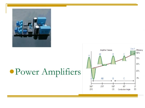
d)According to the method of operation • Class A The output signal varies for a full 360 of the cycle. • Class B A class B circuit provides an output signal varying over one-half the input signal cycle, or for 180 of signal. The dc bias point for class B is therefore at 0V, with the output then varying from this bias point for a half-cycle. • Class AB For class AB operation the output signal swing occurs between 180 and 360 and is neither class A nor class B operation. Class AB operation still requires a push-pull connection to achieve a full output cycle, but the dc bias level is usually closer to the zero base current level for better power efficiency. • Class C The output of a class C amplifier is biased for operation at less than 180 of the cycle and is used in special areas of tuned circuits, such as radio or communications. • Class D This operating class is a form of amplifier operation using pulse (digital) signals which are on for a short interval and off for a longer interval. Using digital techniques makes it possible to obtain a signal that varies over the full cycle (using sample-and-hold circuitry) to create the output from many pieces of input signal. The major advantage of class D operation is that the amplifier is on (using power) only for short intervals and the overall efficiency can practically be very high.
Amplifier Efficiency • The power amplifier efficiency of an amplifier, defined as the ratio of power output to power input, improves (gets higher) going from class A to class D. In general terms we see that a class A amplifier, with dc bias at one-half the supply voltage level, uses a good amount of power to maintain bias, even with no input signal applied. This results in very poor efficiency, especially with small input signals, when very little ac power is delivered to the load. In fact, the maximum efficiency of a class A circuit, occurring for the largest output voltage and current swing, is only 25 % with a direct or series-fed load connection, and 50% with a transformer connection to the load. Class B operation, with no dc bias power for no input signal, can be shown to provide a maximum efficiency that reaches 78.5%. Class D operation can achieve power efficiency over 90% and provides the most efficient operation of all the operating classes. Since class AB falls between class A and class B in bias, it also falls between their efficiency ratings-between 25% (or 50%) and 78.5%.
Series-fed Class A amplifier • This circuit is not the best to use as a large-signal amplifier because of its poor power efficiency. • The power into an amplifier is provided by the supply. With no input signal the dc current drawn is the collector bias current, ICQ. The power then drawn from the supply is Pi(dc) = VCC ICQ • Even with an ac signal applied, the average current drawn from the supply remains the same, so that Pi represents the input power supplied to the class A series-fed amplifier.
5.2 Class B amplifier operation • As the transistor conducts current for only one-half of the signal cycle, it is necessary to use two transistors and have each conduct on opposite half-cycles to obtain output for the full cycle of signal. • Since one part of the circuit pushes the signal high during one half-cycle and the other part pulls the signal low during the other half-cycle, the circuit is referred to as a push-pull circuit.
Power Calculations • Input (dc) Power • Pi(dc) = VCCIdc Where Idc is the average or dc current drawn from the power supplies. • Idc = (2/) I(p) Where I(p) is the peak value of the output current waveform. • Input power is given by Pi(dc) = VCC[(2/) I(p)] • Output (ac) Power P0(ac) = V2L(rms) / RL P0(ac) = V2L(p-p) / 8RL = V2L(p) / 2RL The larger the rms or peak output voltage, the larger the power delivered to the load. • Efficiency • % = P0(ac) / Pi(dc) x 100% = [V2L(p)/2RL] / VCC[(2/) I(p)] x 100% = (/4) [VL(p)/VCC] x 100% • This equation shows that the larger the peak voltage, the higher the circuit efficiency, up to a maximum value when VL(p) = VCC, this maximum efficiency then being • Maximum efficiency = /4 x 100% = 78.5%
Example • For a class B amplifier providing a 20 V peak signal to a 16 load (speaker) and a power supply of VCC = 30 V, determine the input power, output power, and circuit efficiency. • Solution • A 20 V peak signal across a 16 load provides a peak load current of IL(p) = VL(p)/RL = 20 V/16 = 1.25 A • The dc value of the current drawn from the power supply is then Idc = 2/ IL(p) = 2/ (1.25 A) = 0.796 A • and the input power delivered by the supply voltage is Pi(dc) = VCCIdc = (30 V)(0.796 A) = 23.9 W • The output power delivered to the load is P0(ac) = V2L(p)/2RL = (20 V)2/2(16 ) = 12.5 W • for a resulting efficiency of % = P0(ac)/Pi(dc) x 100% = 12.5 W/23.9 W x 100% = 52.3%
Class B Amplifier Circuits • A number of circuit arrangements for obtaining class B operation are possible. The input signal to the amplifier could be a single signal, the circuit then providing two different output stages, each operating for one-half the cycle. If the input is in the form of two opposite polarity signals, two similar stages could be used, each operating on the alternate cycle because of the input signal. One means of obtaining polarity or phase inversion is using a transformer. Opposite polarity inputs can easily be obtained using an op-amp having two opposite outputs, or using a few op-amp stages to obtain two opposite polarity signals. An opposite polarity operation can also be achieved using a single input and complementary transistors.
Complementary-Symmetry Circuits • Using complementary transistors (npn and pnp) it is possible to obtain a full cycle output across a load using half-cycles of operation from each transistor
Crossover Distortion • During a complete cycle of the input a complete cycle of output signal is developed across the load. One disadvantage with the complementary circuit is shown in the resulting crossover distortion in the output signal. Crossover distortion refers to the fact that during the signal crossover from positive to negative (or vice versa) there is some nonlinearity in the output signal. This results from the fact that the circuit does not provide exact switching of one transistor off and the other on at the zero-voltage condition. Both transistors may be partially off so that the output voltage does not follow the input around the zero voltage condition. Biasing the transistors in class AB improves this operation by biasing both transistors to be on for more than half a cycle.
The effect of crossover distortion on sine-wave input • There exists a range of Vi centered around zero where both transistors are cut off and output voltage is zero. This dead band results in the crossover distortion. The effect of crossover distortion is more pronounced when the amplitude of the input signal is small. Crossover distortion in audio power amplifiers gives rise to unpleasant sounds.
Reducing Crossover Distortion • The crossover distortion of a class B output stage can be reduced subtantially employing a high-gain op amp and overall negative feedback, as shown in fig 5.11. The 0.7 V dead band is reduced to 0.7/A0 volts, where A0 is the dc gain of the op amp • Neverthless, the slew-rate limitation of the op amp will cause the alternate turning on and off of the output transistors to be noticeable, especially at high frequencies. A more practical method for reducing and almost eliminating crossover distortion is found in the class AB operation.
Class AB operation • Biasing the complimentary output transistors at a small, non-zero current can eliminate crossover distortion. This can be achieved by applying a bias voltage VBB between the bases of QN and QP, resulting in class AB stage. • For vI = 0, vo = 0 and a voltage VBB /2 appears across the base-emitter junction of each QN and QP. Assuming matched devices, iN = iP = IQ = Is e(VBB / 2VT) the value of VBB is selected so as to yield the required quiescent current IQ. • The class AB stage operates in much the same manner as the class B circuit, with one important exception: For small vI, both transistors conduct, and as vI is increased or decreased, one of the two transistors takes over the operation. Since the transition is a smooth one, crossover distortion will be almost totally eliminated.
Biasing the Class AB Circuit Using Diodes • The figure shows a class AB circuit in which the bias voltage VBB is generated by passing a constant current Ibias through a pair of diodes, or diode-connected transistors, D1 and D2. • Though the crossover distortion is eliminated in this type of configuration, the characteristics doesn’t pass through the origin, and so, with vI = 0, v0 0. Usually, power amplifier being the last stage of the circuit, vI is obtained from the level shifting stage, and the quiescent value of vI can be set at –VBE so as to obtain v0 = 0 with no input signal.
IC power amplifiers LM384 frequency range : 300 kHz Amplification : 34 dB Power rating : 5 W TDA2020 frequency range : 10 Hz to 160 kHz Amplification : 30 dB Power rating : 20 W Advantages of class B operation greater power output less distortion (using a pair of class B) higher efficiency negligible power loss at no signal
5.4 Tuned Power Amplifiers • Tuned amplifiers amplify selective frequency only, using LC network and hence are useful in receivers. The response of tuned amplifier is similar to bandpass filter, with center frequency wo. Tuned amplifiers find application in the radio frequency (RF) and intermediate-frequency (IF) sections of communications receivers and in variety of other systems. • The response is characterized by the center frequency w0, the 3-dB bandwidth B, and the skirt selectivity, which is usually measured as the ratio of the 30-dB bandwidth to the 3-dB bandwidth. In many applications, the 3-dB bandwidth is less than 5% of w0.
The Basic Principle • The basic principle underlying the design of tuned amplifiers is the use of a parallel LCR circuit as the load, or at the input, of a BJT or a FET amplifier. This is shown in with a MOSFET amplifier having a tuned-circuit load. Since this circuit uses a single tuned circuit, it is known as a single-tuned amplifier. The amplifier equivalent circuit is also shown in figure. Here R denotes the parallel equivalent of RL and the output resistance r0 of the FET, and C is the parallel equivalent of CL and the FET output capacitance (usually very small).
Derivations • From the equivalent circuit we can write V0 = -gmVi/YL = -gmVi/(sC + 1/R + 1/sL) YL Vo = -gm Vi or, Vo = (-gm Vi) / ( sC + 1/R + 1/sL) Thus the voltage gain can be expressed as Vo / Vi = - (gm / C) [s / (s2 + s(1/CR) + 1/LC] Transfer function of a bandpass filter is given by T(s) = n2 s / [s2 + s(wo/Q) + wo2] Comparing with the transfer function of BPF Wo = 1 / LC B = 1 / CR Q = wo / B = woCR And center frequency gain Vo / Vi at wo is equal to –gm R
Example • It is required to design a tuned amplifier of the type shown in fig 5.14, having f0 = 1 MHz, 3-dB bandwidth = 10 kHz, and center-frequency gain = -10 V/V. The FET available has at the bias point gm = 5mA/V and r0 = 10k. The output capacitance is negligibly small. Determine the values of RL, CL, and L. • Solution • Center-frequency gain = -10 = -5R. Thus R = 2k. Since R = RL ||r0, then RL = 2.5k. • B = 2 x 104 = 1/CR Thus C = 1/(2 x 104 x 2 x 103) = 7958 pF • Since w0 = 2 x 106 = 1 / LC, we obtain L = 1/(42 x 1012 x 7958 x 10-12) = 3.18 H.
Use of Transformers In many cases it is found that the required value of inductance is not practical, in the sense that coils with required inductance might not be available with the required high values of Q0. A simple solution is to use a transformer to effect an impedance change. Alternatively, a tapped coil, known as an autotransformer, can be used, as shown in figure. Provided the two parts of the inductor are tightly coupled, which can be achieved by winding it on a ferrite core, the transformation relationships shown hold. For example, if a turns ratio n = 3 is used in the amplifier of above example, then a coil with inductance L' = 9 x 3.18 = 28.6 H and a capacitance C' = 7958/9 = 884 pF will be required. Both of these values are more practical than the original ones.
Synchronous Tuning • The 3-dB bandwidth B of the overall amplifier is related to that of the individual tuned circuits, w0/Q, by B = w0/Q (21/N - 1)1/2 • The factor (21/N - 1)1/2 is known as the bandwidth-shrinkage factor. Given B and N, we can determine the bandwidth required of the individual stages.
Stagger-Tuning • While synchronously tuned circuit is used for sharp selectivity confined to a particular frequency, stagger-tuned amplifiers are usually designed so that the overall response exhibits maximal flatness around the center frequency f0.
5.5 Power dissipation consideration • While integrated circuits are used for small-signal and low-power applications, most high-power applications still require individual power transistors. Improvements in production techniques have provided higher power ratings in small-sized packaging cases, have increased the maximum transistor breakdown voltage, and have provided faster-switching power transistors. • The maximum power handled by a particular device and the temperature of the transistor junctions are related since the power dissipated by the device causes an increase in temperature at the junction of the device. • For many applications the average power dissipated may be approximated by PD = VCEIC • This power dissipation, however, is allowed only up to a maximum temperature. For this reason, good heat sinks must be used with these power transistors. • When the heat sink is used, the heat produced by the transistor dissipating power has a larger area from which to radiate (transfer) the heat into the air, thereby holding the case temperature to a much lower value than would result without heat sink. Even with an infinite heat sink, for which the case temperature is held at the ambient (air) temperature, the junction will be heated above the case temperature and a maximum power rating must be considered.