Download
1 / 1
10 likes | 216 Vues
Crystal Growth and the Characterization of Microstructures. Dr. Yan Xin Associate Scholar/Scientist Magnet Science & Technology National High Magnetic Field Laboratory Tallahassee, FL. Rasheedah Muhammad Instructor Holmes Elementary School Miami, FL. Erin Smidt Science Teacher

E N D
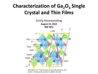
Crystal Growth and the Characterization of Microstructures Dr. Yan Xin Associate Scholar/Scientist Magnet Science & Technology National High Magnetic Field Laboratory Tallahassee, FL RasheedahMuhammad Instructor Holmes Elementary School Miami, FL Erin Smidt Science Teacher Deerlake Middle School Tallahassee, FL Copper is a very good conductor. It is used at the NHMFL in the resistive permanent magnets. Our goal has been to obtain a higher strength and higher conductivity material for the Florida Bitter plates. This will provide a higher magnetic field for the permanent magnets. In pure metal, the properties of the materials are related to the grain sizes. We studied the grain size of different copper samples to determine their strengths. The smaller the grain size of Cu the stronger the copper sample is . To reduce the grain sizes one can fabricate the materials by the bottom-up approach. . Introduction In pure metal, the properties of the materials are related to the grain sizes . The purpose of our project is to evaluate copper grain size to determine the strength of the copper sample. The smaller the grain size the stronger the material. Also, precise methods in sample preparation are needed to produce the optimum surface for observation. Image J Analysis program was used to determine specific grain size. Grains are crystalline in structure. We grew crystals in order to utilize the advanced microscopy techniques to study the microstructures of the crystals. Native copper (~4 cm in size) Process We began our investigation by gathering 0.5 grams of Nickel Carbonate and mixing it with 11 mLof a sulfuric acid solution. After leaving it overnight several small crystals of various shapes and sizes formed. Process A Copper sample is first created in a DC magnetron sputtering machine. The sample is deposited by the bottom-up approach. The material made by deposition is atoms of copper layered on top of one another on a substrate made of Coballt-Molybdenum-Nickel-CromiumAlloy. This thin film (10 microns thick) is grown in 5 m Torr under Ar. After growing a sample through Physical Vapor Deposition in the DC magnetron sputtering machine we examined the refined Cu microstructure on the optical microscope and the surface morphology of the grains on the SEM. Florida Bitter Plates Erin using the optical microscope to capture images of the crystal Rasheedah (above) and Erin (right) in the lab mixing chemicals to grow crystals Nickel Carbonate crystal To get a better understanding of the crystals and their structure we used an optical microscope to inspect the crystals and capture images. Results We observed the plain (flat) view and a cross section of the copper sample. On the plain view no feature was observed on the side of the substrate. A polycrystalline feature was observed in the deposited side. We found the grain size to be about 150 to 200 nm. On the cross-section view colony growth was observed . Polycrystalline features and some twins were observed as well. TEM where images were taken Images of Nickel Carbonate crystal taken on optical microscope (100x) Next, we used the Scanning Electron Microscope (SEM) to get a closer view of the surface of the crystals. The Carl Zeiss 1540 EsB is a field emission SEM with a resolution of 1-2 nm. The images were taken at 7kV using secondary electron SE2 detector. We also used a 200kV transmission electron microscope to look at the crystal. The TEM can magnify the microstructure to 1.5 million times.A TEM works much like a slide projector. A projector shines a beam of light through (transmits) the slide, as the light passes through it is affected by the structures and objects on the slide. These effects result in only certain parts of the light beam being transmitted through certain parts of the slide. This transmitted beam is then projected onto the viewing screen, forming an enlarged image of the slide. Whatever part is transmitted is projected onto a phosphor screen for the user to see. SEM Microscope Copper Sample magnified 20x Using optical microscope SEM Copper SSample Cross sectional view of Cu sample on SEM Rasheedah and Dr. Xin polishing Copper sample to prepare for the SEM SEM Images of Nickel Carbonate Crystal SEM image of Cu grains References Anderoglu, O. "Epitaxial nanotwinned Cu films with high strength and high conductivity." Applied Physics Letters. 93. (2008): Print. Bonetti, E. . "The Influences of Grain Size on the Mechanical Properties of NanocrystalllineAluminium." NanoStructured Materials. 9. (1997): 611-614. Print. Acknowledgements RasheedahMuhammad and Erin Smidt wish to express their sincere gratitude to Dr. Yan Xin, Associate scholar/ Scientist, Dr. Pat Dixon, Director RET Program, and Mr. Jose Sanchez, Assistant Director, RET Program, for their endearing support during the 2010 RET program. Image of Nickel Carbonate crystal on TEM Energy dispersive x-ray spectrum of Nickel Carbonate crystal