Charge Multiplication in Si Sensors
330 likes | 481 Vues
Charge Multiplication in Si Sensors.

Charge Multiplication in Si Sensors
E N D
Presentation Transcript
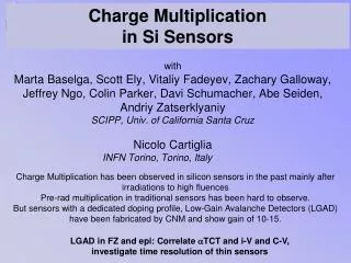
Charge Multiplication in Si Sensors Hartmut F.W. Sadrozinski withMarta Baselga, Scott Ely, VitaliyFadeyev, Zachary Galloway, Jeffrey Ngo, Colin Parker, Davi Schumacher, Abe Seiden, AndriyZatserklyaniySCIPP, Univ. of California Santa CruzNicolo CartigliaINFN Torino, Torino, Italy Charge Multiplication has been observed in silicon sensors in the past mainly after irradiations to high fluences Pre-rad multiplication in traditional sensors has been hard to observe. But sensors with a dedicated doping profile, Low-Gain Avalanche Detectors (LGAD) have been fabricated by CNM and show gain of 10-15. LGAD in FZ and epi: Correlate TCT and i-V and C-V, investigate time resolution of thin sensors
Charge Collection with a’s from Am(241) Am(241) illuminating the back side, range ~ few um’s “electron injection” signal drifts and is then amplified in high field a’s Colin Parker Fast signals! Observed rise times ≈ 400 ps allowing time-resolved current transient (TCT) analysis . Don’t know yet where the lower limit is, since we are still improving the BW of the system. Hartmut F.-W. Sadrozinski, LGAD RD50 Nov 2013
High BW TCT Set-up To understand fast signals need high BW set-up (ex Gregor) Hartmut F.-W. Sadrozinski, LGAD RD50 Nov 2013
Some current transients from alphas on front of new epi sensors look dominated by an RC discharge, let’s investigate what could be the source. Influence of RC Circuit on Pulse TailCoilin Parker (in Appendix) Hartmut F.-W. Sadrozinski, LGAD RD50 Nov 2013
Pulse – shape analysis with TCT Two LGAD from Pablo’s fabrication run W8-C8 and W7I4 are compared as a function of bias with a diode without gain Hartmut F.-W. Sadrozinski, LGAD RD50 Nov 2013
Pulse – shape analysis with TCT e- & h+ from multiplication Initial e- & h+ Hartmut F.-W. Sadrozinski, LGAD RD50 Nov 2013
Initial Pulse charge Correction : from fraction of no-gain pulse beyond time cut: W8-C8 = 1.13 W7-I4 = 1.06 Hartmut F.-W. Sadrozinski, LGAD RD50 Nov 2013
Total charge & initial Pulse charge The initial pulse charge is identical for two different LGAD’s (after correction) and a no-gain diode: Reflects the initial electron drift. Initial pulse charge and total charge for the 3 devices.: G(W8-C8)/G(W7-I4) ≈ 4 at 1000V bias. Hartmut F.-W. Sadrozinski, LGAD RD50 Nov 2013
Doping Concentration from C-V 1/C2 shows a voltage “lag” (“foot”) for the depletion of the p+ layer responsible for multiplication. Use this data to extract an estimate of the doping concentration. Depletion depth x = A/C shows the voltage “lag” for the gain diode Hartmut F.-W. Sadrozinski, LGAD RD50 Nov 2013
Correlation Gain – p-dose G(W8-C8)/G(W7-I4) ≈ 4 at 1000V bias. Given that W8-C8 has much lower current than W7-I4, the data do not support the notion that the leakage current scales with the gain. This means that other effects have much larger effects on the leakage current besides the gain. The gain is influenced by the p-dose in the multiplication layer, where higher gain is correlated with higher p-dose, as expected from simulations. Hartmut F.-W. Sadrozinski, LGAD RD50 Nov 2013
Gain = (total collected charge)/(corr. Initial charge) Even at the low bias voltage of 90V, we observe a gain G=6 for W8-C8. Difference in P+ dose: 20% Hartmut F.-W. Sadrozinski, LGAD RD50 Nov 2013
50um epi 4mm Diode 1/C2 shows thecharacteristic “foot” forgaindiodes Hartmut F.-W. Sadrozinski, LGAD RD50 Nov 2013
TCT fromFront 50um epi 4mm Diode • N.B. • TCT from Back in FZ • Initial Pulse Char. • ~120fC Hartmut F.-W. Sadrozinski, LGAD RD50 Nov 2013
TCT fromFront 50um epi 4mm Diode No-gain Pulse distribution ~independent of bias Gain: Verylarge pulses at 500V bias: gainorbreakdown? Hartmut F.-W. Sadrozinski, LGAD RD50 Nov 2013
Issues with 50um epiStrips • Lowbreakdownvoltages • Diodeneeded 500V (?), strips break down at <200V • No comparisonwith non-gainparts (coming) • Onlypartialcoveragewith p+ implant (select AC7-AC9) • Scanwith x-rays at Diamond (Glasgow) Hartmut F.-W. Sadrozinski, LGAD RD50 Nov 2013
Conclusions on LGAD TCT on FZ LGAD fromthe back-side shows gain up to 14. TCT on FZ LGAD fromthe back-side shows gainat a bias as low as 90V Gainin FZ LGAD isassociatedwith p+ dose, notwithexcessivecurrent. Epi 50um diodesmightexhibitgain at 500V (Front data) Epi 50um stripshavelowbreakdown. Epi 50um stripshaveonlylimitedcoverageby p+ implant. Thinsensorshavehighratecapability and reduce dependence of noiseonexcessleakagecurrent. Hartmut F.-W. Sadrozinski, LGAD RD50 Nov 2013
Fast Rise Time Sensors for Timing • Why thin sensors for fast timing? Thin sensors allow fast rise time because of the fast collection time. But their S/N is reduced. • Why not use thick sensors, and collect only the early part of the electrons or integrate the charge over longer time, reduce noise and trigger low on the rising pulse, like in LHC pixel sensors? • In general: induced pulse development is fairly complicated (i.e. bipolar pulses in neighboring strips, possibility of increased “cross-talk”) so shaping at the collection time seems to be a safe thing to do. • Time resolution due to noise and time walk (amplitude dispersion of Landau): • Assume pulse of amplitude S with dispersionDS/S,electronic noise RMS Nand rise time : • = 0.16 – 0.4 S. Meroli, D. Passeri and L. Servoli, “Energy loss measurement for charged particles invery thin silicon layers”, 11 JINST 6 P06013, 2011. Hartmut F.-W. Sadrozinski, LGAD RD50 Nov 2013
Timing Resolution In the following, the rise time = shaping time will be set equal to the collection time to get optimal performance. This correlates the rise time and the sensor thickness. (i.e. =6.5 ns for 300 µm, . = 1 ns for 50 µm,= 200 ps for 9 µm) For ATLAS type pixels a noise N=1000e- at a shaping time of 500 ps, and the noise scaling like 1/√τR with the shaping time. These assumptions are consistent with the measured noise on the ATLAS pixels the threshold be set at 10 times noise RMS to suppress noise counts Sthr=10*N (iv) a reduction of time walk by a factor CFD due to the use of a constant fraction discriminator , . For high-rate sensors, we look for the fastest rise time with a realistic S/N >30. Then the time resolution depends on the gain as shown in Table 1, with a marked improvement with the use of a constant fraction discriminator even with a modest CFD = 1/3. For a gain G=10, a rise time of =800ps and a sensor thickness of 36µm the time resolution will be 30 - 40ps. Hartmut F.-W. Sadrozinski, LGAD RD50 Nov 2013
Rise Time, Thickness, S/N, Time Resolution Need S/N > 30 CDF = 1/10 Hartmut F.-W. Sadrozinski, LGAD RD50 Nov 2013
Excess Noise in Sensors with Gain Charge multiplication in silicon sensors allows increasing the signal-to-noise ratio S/N as long as the excess noise due to the multiplication process is small. (M. Mikuz, HSTD9, Sept. 2013) F(G=1) =1, F(G1) =2 (R. J. McIntyre, IEEE TED13(1966)164) For LGAD: Current igen = 10 µA/cm2 -> current per pixel i=1nA , =0.1nA Gain = 10, F=2 -> excess Noise at τ=800 ps: 14 e- -> extcess Noise at τ= 20 ns : 70 e- ENC=G Hartmut F.-W. Sadrozinski, LGAD RD50 Nov 2013
Conclusions on Timing Shaping at the collection time correlates sensor thickness. Decisive parameter is S/N. Thin sensors = fast shaping time: Motivator is high rate and low excess noise! Hartmut F.-W. Sadrozinski, LGAD RD50 Nov 2013
Investigating RC sources in the TCT experiment Colin 11/5/13
Some current transients from alphas on front of new epi sensors look dominated by an RC discharge, let’s investigate what could be the source. Intro Hartmut F.-W. Sadrozinski, LGAD RD50 Nov 2013
Circuit Diagram • Current Pulse • Sensor modeled as capacitor (measured 33pF) • Bias T model • Bias Filter • Decoupling Cap • Scope readout resistor Hartmut F.-W. Sadrozinski, LGAD RD50 Nov 2013
Shape of Current Pulse • Initial Pulse • Multiplied Holes Hartmut F.-W. Sadrozinski, LGAD RD50 Nov 2013
Output • Discharge ~ few ns!! • Shape consistent w/ observed Hartmut F.-W. Sadrozinski, LGAD RD50 Nov 2013
Sensor C=11pF • If Sensor C 10pF as in FZ 300um thick case we don’t see as much RC Hartmut F.-W. Sadrozinski, LGAD RD50 Nov 2013
Other Important Parameters? Varying L, R, and C parameters for Bias T doesn’t affect output much. Hartmut F.-W. Sadrozinski, LGAD RD50 Nov 2013
Current Pulse w/ No Hole Contribution - If we take out the tail of holes… Hartmut F.-W. Sadrozinski, LGAD RD50 Nov 2013
Input: Electrons Only Current Pulse, No Hole Contribution Hartmut F.-W. Sadrozinski, LGAD RD50 Nov 2013
Output Signals Sensor Cap = 11pF Sensor Cap = 33pF RC ~ 1ns RC ~ 3ns Hartmut F.-W. Sadrozinski, LGAD RD50 Nov 2013
Conclusions • SPICE indicates that the sensor capacitance should be the dominant factor in discharge time. • For our circuitry RC is of order ~ few ns • Bias T seems not to play an important role, neither does bias filter Hartmut F.-W. Sadrozinski, LGAD RD50 Nov 2013
(Extra) FFT of Input Current • SPICE is also capable of FFT’s, which are pretty cool. They can help visualize the frequencies involved in time-domain signals and thus give us an idea of required BW Hartmut F.-W. Sadrozinski, LGAD RD50 Nov 2013