Internal Logic Analyzer Middle presentation-part A
Internal Logic Analyzer Middle presentation-part A. By: Moran Katz and Zvika Pery Mentor: Moshe Porian Dual-semester project Spring 2012. Agenda. Overview Goals Requirements Architecture Data transfer Internal Logic Analyzer Core Generics Registers Write controller Read controller

Internal Logic Analyzer Middle presentation-part A
E N D
Presentation Transcript
Internal Logic AnalyzerMiddle presentation-part A By: Moran Katz and Zvika Pery Mentor: Moshe Porian Dual-semester project Spring 2012
Agenda • Overview • Goals • Requirements • Architecture • Data transfer • Internal Logic Analyzer Core • Generics • Registers • Write controller • Read controller • RAM • Simulations • Schedule
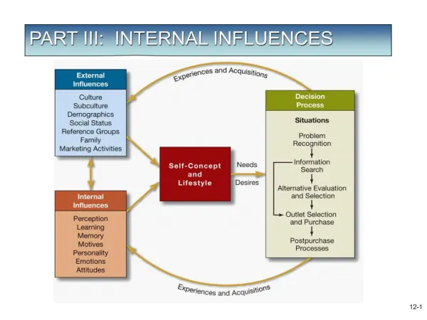
Project Overview Logic Analyzer- Debugging tool for FPGA Contains software & hardware Common Logic Analyzer tools today: Hardware: Change FPGA code Memories to store data Logic to change configuration Software: Include GUI Choose trigger, data location, signals name, record results Altera- Signal Tap Xilinx- Chip Scope
Project goals • Design an internal logic analyzer to the FPGA which will be an independent part • Hardware: (1) VHDL (2) Record the chosen signals (3) Send it back to the user • Software: (1) GUI- allow to present the recorded information (2) Send request to change hardware according user’s choise (3) Build a system to check our implementation Signal Generator UART IN RX PATH TX PATH WBS WBM WBM GUI Internal Logic Analyzer Core 50 MHZ 100 MHZ WhishBone intercon Clock & Reset XILINX- SPARTAN 3E ALTERA- CYCLON II Reset Reset WBS WBS UART OUT WBM WBM- Whishbone Master WBS-Whishbone Slave FPGA Altera Cyclone II
Requirements • Option to choose the parameters • Save the recorded information and present it using waveform • Internal communication is through Wishbone protocol • External communication is through UART protocol Save and load settings Duration of recording position of trigger Type of trigger, for example ‘rise’ Signals name, which signals to record 30%-70% 50%-50% 70%-30%
Architecture Signal Generator UART IN TX PATH RX PATH WBS WBM WBM GUI Internal Logic Analyzer Core 50 MHZ 100 MHZ WhishBone intercon Clock & Reset Reset Reset WBS WBS UART OUT WBM WBM- Whishbone Master WBS-Whishbone Slave FPGA Altera Cyclone II
Data Transfer injecting signals behavior Trigger- first signal Recording time- 50% Signal’s number-2 signal Signal Generator UART IN signal RX PATH TX PATH WBS signal WBM WBM GUI Internal Logic Analyzer Core 50 MHZ 100 MHZ WhishBone intercon Clock & Reset Reset Reset WBS Recorded data WBS UART OUT WBM WBM- Whishbone Master WBS-Whishbone Slave FPGA Altera Cyclone II
The Core • The core have 6 sub blocks: • Write controller. • Read controller. • Registers. • RAM. • WBS. • WBM. Internal Logic Analyzer Core WBS WBM
Generics • The generics contains the basic values of the core’s parts and the configurations of the user. • The generics stay steady during the whole time.
Registers • First we receive the configurations from the user. • we than change the Enable to ‘1’. • From now we raise by one ‘Clk to start’ in every cycle until trigger rise. In the project we have four units of registers: • Trigger type – values between 0-3. defines the type of trigger that we are looking for- {rise, fall, one or zero (for 3 cycles)}. • Trigger position- get values between 0-100. the percentage of the data that will recorded before trigger rise. • clk to start- values 0-256. Saves the number of clock cycles since the system was enabled until trigger rise. • Enable- values 0 or 1. The status of the system, meaning our core starts looking for trigger rise. “000” “001” “011” “010” “11001” “1” 1+ “001”
Write controller • The inputs are the configurations from the registers, and the trigger. • The outputs are the addresses of the relevant data(according to the configuration). • The write controller calculates the address of the relevant data and send it to the read controller . • The Blocks Diagram • In every cycle we get a new trigger and data. • The WC calc the current address and sends it to the RAM. • ALU trigger compare the trigger signal to the relevant configuration. • In case we find a trigger rise, we rise the “trigger found” signal for one cycle. New Trigger Trigger Position ‘1’ Trigger Type Straddr\edaddr Next addr Cuurentaddr Cuurentaddr New Data
Read controller • The Block Diagram • Starts according to trigger rise. • The start and end addresses are being saved, and in every cycle the relevant address is sent to the RAM. • In parallel, data is coming from the RAM and being sent out to the user. • Recieves a start and an end address of the relevant data, that needs to be sent back to the user. • Recieves the data from the RAM and send it to the user via the WBM. START\END ADDR ‘0’ -> ‘1’ Next addr out START\END ADDR Data from the RAM
RAM Input cycle: Output cycle: • The main memory unit. • All the data that’s come as input and needed to be send back to the user is saved in the RAM between that. • Getting the input addtess and data to save. • Sending the output address to the RAM. • Saving the data in the RAM. • The output is the relevant data and the valid signal. • The RAM size is determined according the relevant generics- Enable correct RAM Address enable currect RAM First “word” • For example: • Record_depth_g = 4, • Num_of_signals_g = 5, • Signal_ram_depth_g = 3, • Signal_ram_width_g = 3. '0' '1' First signal Input data Output data output address Valid output Enable correct RAM '0' ‘1’
Simulations • The simulations were done manually in ModelSim. • Generics are at default Values and the input signals were changed in order to check the output. Test 1: trigger rise. trigger position is 0.
Simulations • Test 2: • trigger types: First trigger is fall. Second trigger is ones.
Simulations • Example: Trigger type – rise trigger position - 0 • Example 2: Trigger type – rise trigger position - 50
Schedule 0.5 חן