An Alternative Semiconductor Definition!
An Alternative Semiconductor Definition!. What is a Semiconductor ? B - Ch 1, Y - Ch 1, S - Ch 1. Conductivity/Resistivity Definition ( σ = conductivity, ρ = resistivity) Metals : Good Conductors! 10 3 ≤ σ ≤ 10 8 ( Ω - cm) -1 ; 10 -8 ≤ ρ ≤ 10 -3 Ω - cm

An Alternative Semiconductor Definition!
E N D
Presentation Transcript
What is a Semiconductor?B - Ch 1, Y - Ch 1, S - Ch 1 Conductivity/Resistivity Definition (σ= conductivity,ρ = resistivity) Metals: Good Conductors! 103 ≤σ≤ 108 (Ω-cm)-1; 10-8 ≤ρ≤ 10-3 Ω-cm Semiconductors and Semimetals: 10-8 ≤σ≤ 103 (Ω-cm)-1; 10-3 ≤ρ≤ 108 Ω-cm NOTE THE HUGE RANGE!! Insulators: σ≤ 10-8 (Ω-cm)-1; ρ≥ 108 Ω-cm Actually, there are no rigid boundaries!
Semiconductors Conductivity/Resistivity Definition Metals Semimetals
Semiconductors:Bandgap Definition Semiconductor ~A small bandgap insulator (We’ll define bandgap Eg in detail later). Strictly speaking, it must also be capable of being doped(we’ll define doping in detail later). Typical Bandgaps Semiconductors: 0 ~ ≤ Eg ≤ ~ 3 eV Metals & Semimetals:Eg = 0 eV Insulators:Eg≥3 eV Exception Diamond, with Eg = ~ 6 eV, is usually an insulator, but it can be doped & used as a semiconductor! Also, sometimes there is confusing terminology like GaAs: Eg = 1.5 eV is sometimes called semi-insulating!
Some Semiconductor Characteristics • In pure materials(which are very rare): The electrical conductivity σ exp(cT) T = Kelvin Temperature, c = constant • In impure materials(most materials): • The electrical conductivity σdepends strongly on impurity concentrations. • “Doping” means to add impurities to change σ • The electrical conductivity σ can be changed by light or electron radiation & by injection of electrons at contacts • Transport of charge can occur by the motion of electrons or holes (defined later).
The Best KnownSemiconductor is Silicon (Si) • However, there are HUNDREDS (maybeTHOUSANDS) of others! • Elemental:Si, Ge, C (diamond) • Binary compounds:GaAs, InP, . • Organic compounds:(CH)n (polyacetyline) • Magnetic semiconductors:CdxMn1-xTe, … • Ferroelectric semiconductors:SbI, … • Superconducting compounds (!!) GeTe, SrTiO3, .. ( “High Tc materials!” )
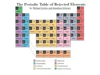
The Periodic Table: The Relevant Parts for Elemental & Binary Semiconductors III IV V VI II II Group IV Materials & III-V & II-VI Compounds
Diamond Lattice Group IVElements III-V, II-VI, & IV-IV Compounds Zincblende or Wurtzite Lattices Diamond (α-Sn or gray tin) Band gap (mostly) decreases & near neighbor distance (mostly) increases within a row going from IV elements to III-V compounds to II-VI compounds. Band gap (mostly) decreases & near neighbor distance (mostly) increases going from IV elements to III-V to II-VI compounds. Band gap (mostly) decreases & nearest neighbor distance (mostly) increases going down a column.
Many Materials of Interest in This Course: Have crystal lattice structures Diamond or Zincblende (These will be discussed in detail again later!) • In these structures, each atom is tetrahedrally coordinated with four (4) nearest-neighbors. • The bonding between neighbors is (mostly) sp3 hybrid bonding (strongly covalent). • There are 2 atoms/unit cell (repeated to form an infinite solid).
The Zincblende (ZnS) Lattice Zincblende Lattice: The Cubic Unit Cell. If all atoms are the same, it becomes the Diamond Lattice! Zincblende Lattice: A Tetrahedral Bonding Configuration
Zincblende & Diamond Lattices Diamond Lattice The Cubic Unit Cell Zincblende Lattice The Cubic Unit Cell Semiconductor Physicists & Engineers need to know these structures!
Diamond Lattice Diamond Lattice The Cubic Unit Cell. Semiconductor Physicists & Engineers need to know these structures!
Zincblende (ZnS) Lattice Zincblende Lattice The Cubic Unit Cell.
Some Materials of Interest in This Course have crystal lattice structures Wurtzite Structure (This will be discussed in detail again later!) • This is similar to the Zincblende structure, but it has hexagonal symmetry instead of cubic. • In these structures, each atom is tetrahedrally coordinated with four (4) nearest-neighbors. • The bonding between neighbors is (mostly) sp3 hybrid bonding (strongly covalent). • There are 2 atoms/unit cell (repeated to form an infinite solid).
Wurtzite Lattice Semiconductor Physicists & Engineers need to know these structures!
Room Temperature Properties of Some Important Semiconductor Materials

