Semiconductor diodes
Semiconductor diodes. Lecture 3. Discrete Semiconductor Devices. Semiconductor Materials Conductor and Insulators. N-type, P-Type, electron, and hole current PN junction, depletion region, potential barrier. Diodes General Purpose Diodes Light Emitting Diodes Zener Diodes Photo Diodes.

Semiconductor diodes
E N D
Presentation Transcript
Semiconductor diodes Lecture 3 Muhammad Amir Yousaf
Discrete Semiconductor Devices • Semiconductor Materials • Conductor and Insulators. • N-type, P-Type, electron, and hole current • PN junction, depletion region, potential barrier. • Diodes • General Purpose Diodes • Light Emitting Diodes • Zener Diodes • Photo Diodes • After this lecture, you should be able to: • Use a diode in common applications. • Forward bias: • Required condition • Effect on depletion region • Barrier potential and it effects • Reverse bias: • Required condition • Reverse current and reverse breakdown Muhammad Amir Yousaf
Conductor and Insulators.Atomic Model • the gap can be crossed • only when breakdown • conditions occur the gap is smaller and can be crossed when a photon is absorbed the conduction band and valence band overlap, so there is no gap Muhammad Amir Yousaf
Silicon and Germanium Muhammad Amir Yousaf
Conduction Electron and Holes. An intrinsic (pure) silicon crystal at room temperature has sufficient heat energy for some valence electrons to jump the gap from the valence band into the conduction band, becoming free electron called ‘Conduction Electron’ It leaves a vacancy in valance band, called hole. Recombination occurs when a conduction-band electron loses energy and falls back into a hole in the valence band. Muhammad Amir Yousaf
Electron Hole Current. In conduction band : When a voltage is applied across a piece of intrinsic silicon, the thermally generated free electrons in the conduction band, are now easily attracted toward the positive end. This movement of free electrons is one type of current in a semiconductive material and is called electron current. In valance band: In valance band holes generated due to free electrons. Electrons in the valance band are although still attached with atom and not free to move, however they cam move into nearby hole with a little change in energy, thus leaving another hole where it came from. Effectively the hole has moved from one place to another in the crystal structure. It is called hole current. Muhammad Amir Yousaf
Electron Hole Current. Muhammad Amir Yousaf
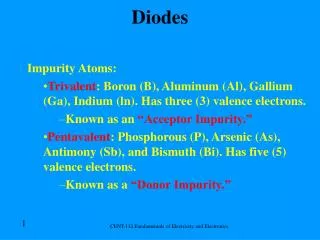
N-type semiconductor Electrons in the conduction band and holes in the valence band make the semiconductive material to conduct but they are too limited to make it a very good conductor.. Adding impurities in materials like Si or Ge can drastically increase the conductivity of material. The process is called doping. Addition of a penta-valent material icnreases the number of conduction electrons. Majority carrier: electrons Minority carriers: holes Material is called N-type semiconductor An antimony (Sb) impurity atom is shown in the center. The extra electron from the Sb atom becomes a free electron. Muhammad Amir Yousaf
P-type semiconductor. Trivalent impurity atom in a silicon crystal structure. A boron (B) impurity atom is shown in the center. Muhammad Amir Yousaf
PN Junction Although P-type material has holes in excess and N-type material has a number of free conduction electron however the net number of proton and electron are equal in each individual material keeping it just neutral. The basic silicon structure at the instant of junction formation showing only the majority and minority carriers. Free electrons in the n region near the pn junction begin to diffuse across the junction and fall into holes near the junction in the p region. Muhammad Amir Yousaf
PN Junction For every electron that diffuses across the junction and combines with a hole, a positive charge is left in the n region and a negative charge is created in the p region, forming a barrier potential. This action continues until the voltage of the barrier repels further diffusion. The blue arrows between the positive and negative charges in the depletion region represent the electricfield. Muhammad Amir Yousaf
Energy band and potential barrier Muhammad Amir Yousaf
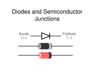
Diodes • Diode, semiconductor material, such as silicon, in which half is doped as p-region and half is doped as n-region with a pn-junction in between. • The p region is called anode and n type region is called cathode. Diode symbol Muhammad Amir Yousaf
Diodes • Diode, semiconductor material, such as silicon, in which half is doped as p-region and half is doped as n-region with a pn-junction in between. • The p region is called anode and n type region is called cathode. • It conducts current in one direction and offers high (ideally infinite) resistance in other direction. Diode symbol Muhammad Amir Yousaf
Forward Biased • Forward bias is a condition that allows current through pn junction. • A dc voltage (Vbais) is applied to bias a diode. • Positive side is connected to p-region (anode) and negative side is connected with n-region. • Vbais must be greater than ‘barrier potential’ As more electrons flow into the depletion region reducing the number of positive ions and similarly more holes move in reducing the positive ions. This reduces the width of depletion region. Current limiting resistance Muhammad Amir Yousaf
Reverse Biased • Reverse bias is a condition that prevents current through junction. • Positive side of Vbias is connected to the n-region whereas the negative side is connected with p-region. • Depletion region get wider with this configuration. The positive side of bias voltage attracts the majority carriers of n-type creating more positive ions at the junction. This widens the depletion region. Muhammad Amir Yousaf
Reverse Current • A small amount current is generated due to the minority carriers in p and n regions. • These minority carriers are produced due to thermally generated hole-electron pairs. • Minority electrons in p-region pushed towards +ve bias voltage, cross junction and then fall in the holes in n-region and still travel in valance band generating a hole current. Muhammad Amir Yousaf
Reverse Breakdown • If the external bias voltage is increased to a value call breakdown voltage the reverse current can increase drastically. • Free minority electrons get enough energy to knock valance electron into the conduction band. • The newly released electron can further strike with other atoms. • The process is called avalanche effect. Muhammad Amir Yousaf
Diode V-I Characteristic • VI Characteristic for forward bias. • The current in forward biased called forward current and is designated If. • At 0V (Vbias) across the diode, there is no forward current. • With gradual increase of Vbias, the forward voltage and forward current increases. • A resistor in series will limit the forward current in order to protect the diode from overheating and permanent damage. • A portion of forward-bias voltage drops across the limiting resistor. • Continuing increase of Vf causes rapid increase of forward current but only a gradual increase in voltage across diode. Muhammad Amir Yousaf
Diode V-I Characteristic • Dynamic Resistance: • The resistance of diode is not constant but it changes over the entire curve. So it is called dynamic resistance. Muhammad Amir Yousaf
Diode V-I Characteristic • VI Characteristic for reverse bias. • In reverse-bias voltage, there is only a small current through the junction. • There is only a small voltage cross the diode and small current through it as we increase the applied reverse voltage. • At a point, reverse current shoots up with the break down of diode. The voltage called break down voltage. This is not normal mode of operation. • After this point the reverse voltage remains at approximately VBR but IR increase very rapidly. • Break down voltage depends on doping level, set by manufacturer. Muhammad Amir Yousaf
Diode V-I Characteristic • The complete V-I characteristic curve Muhammad Amir Yousaf
Diode models • Ideal Diode Model • Barrier potential, the forward dynamic resistance and reverse current all are neglected. Muhammad Amir Yousaf
Diode models VF = 0.7V • Practical Diode Model • Barrier potential, the forward dynamic resistance and reverse current all are neglected. • Forward current IF is determined using Kirchhoff’s voltage as follows: Kent Bertilsson Muhammad Amir Yousaf
Half wave Rectifiers • As diodes conduct current in one direction and block in other. • When connected with ac voltage, diode only allows half cycle passing through it and hence convert ac into dc. • As the half of the wave get rectified, the process called half wave rectification. • A diode is connected to an ac source and a load resistor forming a half wave rectifier. • Positive half cycle causes current through diode, that causes voltage drop across resistor. Muhammad Amir Yousaf
Diode as Rectifiers • Reversing diode. • Average value of Half wave output voltage: VAVG = VP / pi • VAVG is approx 31.8% of Vp • PIV: Peak Inverse Voltage = Vp Muhammad Amir Yousaf
Full wave rectifiers • A full wave rectifier allows unidirectional current through the load during the entire 360 degree of input cycle. • The output voltage have twice the input frequency. • VAVG is 63.7% of Vp Full Wave Rectifier VAVG = 2VP / pi Muhammad Amir Yousaf
The Center-Tapped Full wave rectifiers • A center-tapped transformer is used with two diodes that conduct on alternating half-cycles. During the positive half-cycle, the upper diode is forward-biased and the lower diode is reverse-biased. During the negative half-cycle, the lower diode is forward-biased and the upper diode is reverse-biased. Muhammad Amir Yousaf
The Bridge Full-wave rectifiers • The Bridge Full-Wave rectifier uses four diodes connected across the entire secondary as shown. Conduction path for the positive half-cycle. Conduction path for the negative half-cycle. Muhammad Amir Yousaf
The Bridge Full-Wave Rectifier Example: Determine the peak output voltage and current in the 3.3 kW load resistor if Vsec = 24 Vrms. Use the practical diode model. Solution: The peak output voltage is: =32.5 V Applying Ohm’s law, Ip(out) = 9.8 mA Muhammad Amir Yousaf
Zener Diodes • A Zener diode is a silicon pn junction that is designed for operation in reverse-breakdown region • When a diode reaches reverse breakdown, its voltage remains almost constant even though the current changes drastically, and this is key to the Zener diode operation. • Ideally, the reverse breakdown has a constant breakdown voltage. This makes it useful as a voltage reference, which is its primary application. Muhammad Amir Yousaf
Zener Breakdown Characteristic • As the reverse voltage (VR) increases, the reverse current(IR) remains extremely small up to the knee of the curve. • Reverse current is also called Zener current(Iz). • At this point the breakdown effect begins, the internal Zener resistance (ZZ) begins to decrease. • The reverse current increase rapidly. • The Zener breakdown (VZ) voltage remains nearly constant. Muhammad Amir Yousaf
Zener Diode Impedence • The zener impedance, ZZ, is the ratio of a change in voltage in the breakdown region to the corresponding change in current: What is the zener impedance if the zener diode voltage changes from 4.79 V to 4.94 V when the current changes from 5.00 mA to 10.0 mA? Practical model 30 W Muhammad Amir Yousaf
Zener Regulation • The ability to keep the reverse voltage constant across its terminal is the key feature of the Zener diode. • It maintains constant voltage over a range of reverse current values. • A minimum reverse current IZK must be maintained in order to keep diode in regulation mode. Voltage decreases drastically if the current is reduced below the knee of the curve. • Above IZM, max current, the Zener may get damaged permanently. Muhammad Amir Yousaf
Zener Regulation • Zener Regulation with variable input voltage • Ideal model of IN4047A • IZK = 0.25mA • VZ = 10V • PD(max) = 1W, IZM = 1W / 10V = 100mA Muhammad Amir Yousaf
Zener Regulation • Zener Regulation with variable load • It maintains voltage a nearly constant across RL as long as Zener current is within IZK and IZM. Muhammad Amir Yousaf
Zener Diode Applications Zeners can also be used as limiters. The back-to-back zeners in this circuit limit the output to the breakdown voltage plus one diode drop. Question: What are the maximum positive and negative voltages if the zener breakdown voltage is 5.6 V? ± 6.3 V Muhammad Amir Yousaf
Optical Diodes • Light Emitting Diodes (LEDs): Diodes can be made to emit light electroluminescence) or sense light. • When forward biased electrons form n-region cross the junction and recombines to holes with the emission of photons. • Various impurities are added during the doping process to establish the wavelength of the emitted light. • The process is called electroluminescence. Muhammad Amir Yousaf
Optical Diodes • LEDs vary widely in size and brightness – from small indicating lights and displays to high-intensity LEDs that are used in traffic signals, outdoor signs, and general illumination. • LEDs are very efficient light emitters, and extremely reliable, so domain of uses getting wider. Muhammad Amir Yousaf
Photo Diode • A photodiode is a special light sensitive diode with a clear window to the pn junction. It is operated with reverse bias. Reverse current increases with greater incident light. • The tiny current that is present when the diode is not exposed to light is called dark current Dark current Muhammad Amir Yousaf
VaractorDiode • A varactor diode is a special purpose diode operated in reverse-bias to form a voltage-controlled capacitor. The width of the depletion region increases with reverse-bias. • Varactor diodes are used in tuning applications. The applied voltage controls the capacitance and hence the resonant frequency. By varying R2, the reverse bias on D is changed. This changes the capacitance, and hence the resonant frequency. Muhammad Amir Yousaf
Refrences • Electronic Devices by Floyd 9th Edition • Chapter 1,2,3 Muhammad Amir Yousaf