Diodes
Explore diode concepts with circuit symbols, i-v characteristics, rectifier circuits, logic gates, and various models used in microelectronic circuits like ideal, zener, and small-signal models. Study examples and waveforms to grasp diode behaviors effectively.


Diodes
E N D
Presentation Transcript
Diodes 1
Figure 3.1 The ideal diode: (a) diode circuit symbol; (b)i–vcharacteristic; (c) equivalent circuit in the reverse direction; (d) equivalent circuit in the forward direction. Microelectronic Circuits - Fifth Edition Sedra/Smith
Figure 3.2 The two modes of operation of ideal diodes and the use of an external circuit to limit the forward current (a) and the reverse voltage (b). Microelectronic Circuits - Fifth Edition Sedra/Smith
Figure 3.3 (a) Rectifier circuit. (b) Input waveform. (c) Equivalent circuit when vI 0. (d) Equivalent circuit when vI 0. (e) Output waveform. Microelectronic Circuits - Fifth Edition Sedra/Smith
Figure E3.1 Microelectronic Circuits - Fifth Edition Sedra/Smith
Figure E3.2 Microelectronic Circuits - Fifth Edition Sedra/Smith
Figure 3.4 Circuit and waveforms for Example 3.1. Microelectronic Circuits - Fifth Edition Sedra/Smith
Figure 3.5 Diode logic gates: (a) OR gate; (b) AND gate (in a positive-logic system). Microelectronic Circuits - Fifth Edition Sedra/Smith
Figure 3.6 Circuits for Example 3.2. Microelectronic Circuits - Fifth Edition Sedra/Smith
Figure E3.4 Microelectronic Circuits - Fifth Edition Sedra/Smith
Figure E3.5 Microelectronic Circuits - Fifth Edition Sedra/Smith
Figure 3.7 The i–vcharacteristic of a silicon junction diode. Microelectronic Circuits - Fifth Edition Sedra/Smith
Figure 3.8 The diode i–v relationship with some scales expanded and others compressed in order to reveal details. Microelectronic Circuits - Fifth Edition Sedra/Smith
Figure 3.9 Illustrating the temperature dependence of the diode forward characteristic. At a constant current, the voltage drop decreases by approximately 2 mV for every 1C increase in temperature. Microelectronic Circuits - Fifth Edition Sedra/Smith
Figure E3.9 Microelectronic Circuits - Fifth Edition Sedra/Smith
Figure 3.10 A simple circuit used to illustrate the analysis of circuits in which the diode is forward conducting. Microelectronic Circuits - Fifth Edition Sedra/Smith
Figure 3.11 Graphical analysis of the circuit in Fig. 3.10 using the exponential diode model. Microelectronic Circuits - Fifth Edition Sedra/Smith
Figure 3.12 Approximating the diode forward characteristic with two straight lines: the piecewise-linear model. Microelectronic Circuits - Fifth Edition Sedra/Smith
Figure 3.13 Piecewise-linear model of the diode forward characteristic and its equivalent circuit representation. Microelectronic Circuits - Fifth Edition Sedra/Smith
Figure 3.14 The circuit of Fig. 3.10 with the diode replaced with its piecewise-linear model of Fig. 3.13. Microelectronic Circuits - Fifth Edition Sedra/Smith
Figure 3.15 Development of the constant-voltage-drop model of the diode forward characteristics. A vertical straight line (B) is used to approximate the fast-rising exponential. Observe that this simple model predicts VD to within 0.1 V over the current range of 0.1 mA to 10 mA. Microelectronic Circuits - Fifth Edition Sedra/Smith
Figure 3.16 The constant-voltage-drop model of the diode forward characteristics and its equivalent-circuit representation. Microelectronic Circuits - Fifth Edition Sedra/Smith
Figure E3.12 Microelectronic Circuits - Fifth Edition Sedra/Smith
Figure 3.17 Development of the diode small-signal model. Note that the numerical values shown are for a diode with n = 2. Microelectronic Circuits - Fifth Edition Sedra/Smith
Figure 3.18(a) Circuit for Example 3.6. (b) Circuit for calculating the dc operating point. (c) Small-signal equivalent circuit. Microelectronic Circuits - Fifth Edition Sedra/Smith
Figure 3.19 Circuit for Example 3.7. Microelectronic Circuits - Fifth Edition Sedra/Smith
Figure E3.16 Microelectronic Circuits - Fifth Edition Sedra/Smith
Table 3.1 Modeling the Diode Forward Characteristic Microelectronic Circuits - Fifth Edition Sedra/Smith
Table 3.1 (Continued) Microelectronic Circuits - Fifth Edition Sedra/Smith
Figure 3.20 Circuit symbol for a zener diode. Microelectronic Circuits - Fifth Edition Sedra/Smith
Figure 3.21 The diode i–vcharacteristic with the breakdown region shown in some detail. Microelectronic Circuits - Fifth Edition Sedra/Smith
Figure 3.22 Model for the zener diode. Microelectronic Circuits - Fifth Edition Sedra/Smith
Figure 3.23(a) Circuit for Example 3.8. (b) The circuit with the zener diode replaced with its equivalent circuit model. Microelectronic Circuits - Fifth Edition Sedra/Smith
Figure 3.24 Block diagram of a dc power supply. Microelectronic Circuits - Fifth Edition Sedra/Smith
Figure 3.25(a) Half-wave rectifier. (b) Equivalent circuit of the half-wave rectifier with the diode replaced with its battery-plus-resistance model. (c) Transfer characteristic of the rectifier circuit. (d) Input and output waveforms, assuming that rD!R. Microelectronic Circuits - Fifth Edition Sedra/Smith
Figure 3.26 Full-wave rectifier utilizing a transformer with a center-tapped secondary winding: (a) circuit; (b) transfer characteristic assuming a constant-voltage-drop model for the diodes; (c) input and output waveforms. Microelectronic Circuits - Fifth Edition Sedra/Smith
Figure 3.27 The bridge rectifier: (a) circuit; (b) input and output waveforms. Microelectronic Circuits - Fifth Edition Sedra/Smith
Figure 3.28(a) A simple circuit used to illustrate the effect of a filter capacitor. (b) Input and output waveforms assuming an ideal diode. Note that the circuit provides a dc voltage equal to the peak of the input sine wave. The circuit is therefore known as a peak rectifier or a peak detector. Microelectronic Circuits - Fifth Edition Sedra/Smith
Figure 3.29 Voltage and current waveforms in the peak rectifier circuit with CR@T. The diode is assumed ideal. Microelectronic Circuits - Fifth Edition Sedra/Smith
Figure 3.30 Waveforms in the full-wave peak rectifier. Microelectronic Circuits - Fifth Edition Sedra/Smith
Figure 3.31 The “superdiode” precision half-wave rectifier and its almost-ideal transfer characteristic. Note that when vI > 0 and the diode conducts, the op amp supplies the load current, and the source is conveniently buffered, an added advantage. Not shown are the op-amp power supplies. Microelectronic Circuits - Fifth Edition Sedra/Smith
Figure 3.32 General transfer characteristic for a limiter circuit. Microelectronic Circuits - Fifth Edition Sedra/Smith
Figure 3.33 Applying a sine wave to a limiter can result in clipping off its two peaks. Microelectronic Circuits - Fifth Edition Sedra/Smith
Figure 3.34 Soft limiting. Microelectronic Circuits - Fifth Edition Sedra/Smith
Figure 3.35 A variety of basic limiting circuits. Microelectronic Circuits - Fifth Edition Sedra/Smith
Figure E3.27 Microelectronic Circuits - Fifth Edition Sedra/Smith
Figure 3.36 The clamped capacitor or dc restorer with a square-wave input and no load. Microelectronic Circuits - Fifth Edition Sedra/Smith
Figure 3.37 The clamped capacitor with a load resistance R. Microelectronic Circuits - Fifth Edition Sedra/Smith
Figure 3.38 Voltage doubler: (a) circuit; (b) waveform of the voltage across D1. Microelectronic Circuits - Fifth Edition Sedra/Smith
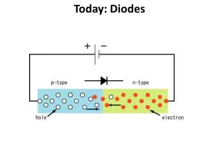
Figure 3.39 Simplified physical structure of the junction diode. (Actual geometries are given in Appendix A.) Microelectronic Circuits - Fifth Edition Sedra/Smith