Ch5 Diodes and Diodes Circuits
480 likes | 998 Vues
Circuits and Analog Electronics. Ch5 Diodes and Diodes Circuits. 5.1 The Physical Principles of Semiconductor 5.2 Diodes 5.3 Diode Circuits 5.4 Zener Diode. References : Floyd-Ch2; Gao-Ch6;. Ch5 Diodes and Diodes Circuits. 5.1 The Physical Principles of Semiconductor. Key Words :

Ch5 Diodes and Diodes Circuits
E N D
Presentation Transcript
Circuits and Analog Electronics Ch5 Diodes and Diodes Circuits 5.1The Physical Principles of Semiconductor 5.2 Diodes 5.3Diode Circuits 5.4Zener Diode References: Floyd-Ch2; Gao-Ch6;
Ch5 Diodes and Diodes Circuits 5.1The Physical Principles of Semiconductor Key Words: Intrinsic(pure) Semiconductors Electrons, Holes, Carriers, Phosphorus Doping (N-type) Boron Doping (P-type) PN Junction
Conductor < 10-4·cm Insulator 1010 · cm Semiconductor • Different types of solids: Si Cu*1011 · cm , Ge Cu*107 · cm • The atomic structure of aneutral silicon atom Valence electrons Valence electrons Ch5 Diodes and Diodes Circuits 5.1The Physical Principles of Semiconductor Intrinsic (pure)Semiconductors
A hole A free electron Ch5 Diodes and Diodes Circuits 5.1The Physical Principles of Semiconductor Intrinsic (pure) Semiconductors • Intrinsic(pure) silicon • An electron-hole pair is created when anelectron get excited by thermal or light energy; • Recombination occurs when an electron loses energy and falls back into a hole.
Both electrons and holes carry current-- carriers. • In intrinsic semiconductors the electron and hole concentrations are equal because carriers are created in pairs • The intrinsic concentration depends exponentially on temperature. • At room temp (300K), the intrinsic carrier concentration of silicon is: Ch5 Diodes and Diodes Circuits 5.1The Physical Principles of Semiconductor Intrinsic (pure) Semiconductors • Holes also conduct current. In reality, it’s the movement of all the other electrons. The hole allows this motion. • Holes have positive charge. • • Current flows in the same direction as the holes move.
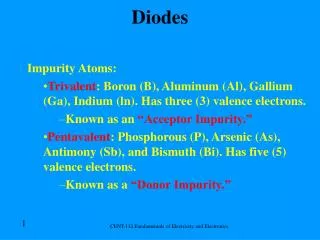
Ch5 Diodes and Diodes Circuits 5.1The Physical Principles of Semiconductor Phosphorus Doping (N-type) • Phosphorus has 5 valence electrons. • • P atoms will sit in the location of a Si atom in the lattice, to avoid breaking symmetry, but each will have an extra electron that does not bond in the same way. And these extra electrons are easier to excite (and can move around more easily) • • These electrons depends on the amounts of the two materials.
Ch5 Diodes and Diodes Circuits 5.1The Physical Principles of Semiconductor Phosphorus Doping (N-type) Electrons---Majority carrier. Holes---Minority carrier Phosphorus---Donor materials. • In equilibrium, • At room temp (300K), if 1/1010 donors are added to the intrinsic silicon, • then the electron carrier concentration is about 1013cm-3; the hole carrier concentration is about 106cm-3. • Phosphorus Intrinsic silicon
Ch5 Diodes and Diodes Circuits 5.1The Physical Principles of Semiconductor Boron Doping (P-type) Holes---Majority carrier;Electrons---Minority carrier Boron---acceptor materials. • Boron has 3 valence electrons. • • B will sit at a lattice site, but the adjacent Si atoms lack an electron to fill its shell. This creates a hole.
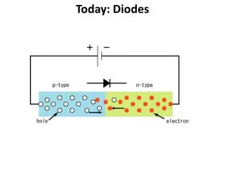
Ch5 Diodes and Diodes Circuits 5.1The Physical Principles of Semiconductor PN Junction • N-type materials: Doping Si with a Group V element, providing extra electrons (n for negative) . • P-type materials: Doping Si with a Group III element, providing extra holes (p for positive). What happens when P-type meets N-type?
Ch5 Diodes and Diodes Circuits 5.1The Physical Principles of Semiconductor PN Junction What happens when P-type meets N-type? • Holes diffuse from the P-type into the N-type, electrons diffuse from the N-type • into the P-type, creating a diffusion current. • • Once the holes [electrons] cross into the N-type [P-type] region, they recombine • with the electrons [holes]. • • This recombination “strips” the n-type [P-type] of its electrons near the • boundary, creating an electric field due to the positive and negative bound • charges. • • The region “stripped” of carriers is called the space-charge region, or depletion • region. • • V0 is the contact potential that exists due to the electric field. Typically, at room • temp, V0is 0.5~0.8V. • • Some carriers are generated (thermally) and make their way into the depletion region where they are whisked away by the electric field, creating a drift current.
Ch5 Diodes and Diodes Circuits 5.1The Physical Principles of Semiconductor PN Junction What happens when P-type meets N-type? • There are two mechanisms by which mobile carriers move in • semiconductors – resulting in current flow • – Diffusion • • Majority carriers move (diffuse) from a place of higher • concentration to a place of lower concentration • – Drift • • Minority carrier movement is induced by the electric field. • In equilibrium, diffusion current (ID) is balanced by drift current (IS). • So, there is no net current flow.
Ch5 Diodes and Diodes Circuits 5.1The Physical Principles of Semiconductor PN Junction Forward bias: apply a positive voltage to the P-type, negative to N-type. Add more majority carriers to both sides shrink the depletion region lower V0 diffusion current increases. • Decrease the built-in potential, lower • the barrier height. • • Increase the number of carriers able to • diffuse across the barrier • • Diffusion current increases • • Drift current remains the same. The • drift current is essentially constant, as • it is dependent on temperature. • • Current flows from p to n
Ch5 Diodes and Diodes Circuits 5.1The Physical Principles of Semiconductor PN Junction Reverse bias: apply a negative voltage to the P-type, positive to N-type. • Increase the built-in potential, increase the barrier height. • • Decrease the number of carriers able to diffuse across the barrier. • • Diffusion current decreases. • • Drift current remains the same • • Almost no current flows. Reverse leakage current, IS, is the drift current, flowing from N to P.
Ch5 Diodes and Diodes Circuits 5.2Diodes Key Words: Diode I-V Characteristic Diode Parameters, Diode Models
Ch5 Diodes and Diodes Circuits 5.2Diodesand Diode Circuits PN Junction Diode V-A Characteristic Typical PN junction diode volt-ampere characteristic is shown on the left. – In forward bias, the PN junction has a “turn on” voltage based on the “built-in” potential of the PN junction. turn on voltage is typically in the range of 0.5V to 0.8V – In reverse bias, the PN junction conducts essentially no current until a critical breakdown voltage is reached. The breakdown voltage can range from 1V to 100V. Breakdown mechanisms include avalanche and zener tunneling.
Ch5 Diodes and Diodes Circuits 5.2Diodesand Diode Circuits PN Junction Diode V-A Characteristic Current Equations • The forward bias current is closely approximated by where VT =kT/q is the thermal voltage (~25.8mV at room temp T= 300K or 27C ) k = Boltzman’s constant = 1.38 x 10⁻²³ joules/kelvin T = absolute temperature q = electron charge = 1.602 x 10⁻¹⁹ coulombs n = constant dependent on structure, between 1 and 2 (we will assume n = 1) IS = scaled current for saturation current that is set by diode size – Notice there is a strong dependence on temperature – We can approximate the diode equation for vD>> VT ,
P5.1, PN Junction when T = 300K,Find iD when Ch5 Diodes and Diodes Circuits 5.2Diodesand Diode Circuits PN Junction Diode V-A Characteristic Current Equations • In reverse bias (when vD << 0 by at least VT), then • In breakdown, reverse current increases rapidly… a vertical line
Ch5 Diodes and Diodes Circuits 5.2Diodesand Diode Circuits PN Junction Diode V-A Characteristic
operating point Q Load line Ch5 Diodes and Diodes Circuits 5.2Diodesand Diode Circuits PN Junction Diode V-A Characteristic P5.2, Look at the simple diode circuit below. ID=7(mA), VD=0.8(V)
Ch5 Diodes and Diodes Circuits 5.2Diodesand Diode Circuits Diode Parameters
Ch5 Diodes and Diodes Circuits 5.2Diodesand Diode Circuits Diodes
Ch5 Diodes and Diodes Circuits 5.2Diodesand Diode Circuits Light Emitting Diodes • When electrons and holes • combine, they release energy. • • This energy is often released as heat into the lattice, but in some materials, they release light. • • This illustration describes the importance of the plastic bubble in directing the light so that it is more effectively seen.
Ch5 Diodes and Diodes Circuits 5.2Diodesand Diode Circuits Diode Models-- The Ideal Switch Model When forward-biased, the diode ideally acts as a closed (on) witch. When reverse-biased, the diode acts as an open (off) switch.
Ch5 Diodes and Diodes Circuits 5.2Diodesand Diode Circuits Diode Models-- The Offset Model VVon,closed switch V< Von, open switch Si diode:Von ≈ 0.7(V)(0.6~0.8) Ge diode:Von ≈ 0.2(V)
Ch5 Diodes and Diodes Circuits 5.2Diodesand Diode Circuits Diode Models--TheSmall-Signal Model Some circuit applications bias the diode at a DC point (VD) and superimpose a small signal (vd(t)) on top of it. Together, the signal is vD(t), consisting of both DC and AC components – Graphically, can show that there is a translation of voltage to current (id(t)) – Can model the diode at this bias point as a resistor with resistance as the inverse of the tangent of the i-v curve at that point
Ch5 Diodes and Diodes Circuits 5.2Diodesand Diode Circuits Diode Models--TheSmall-Signal Model – And if vd(t) is sufficiently small then we can expand the exponential and get an approximate expression called the small- signal approximation (valid for vd < 10mV) – So, the diode small-signal resistance is…
Ch5 Diodes and Diodes Circuits 5.2Diodesand Diode Circuits Diode Models--TheSmall-Signal Model Frequency is not high.
Ch5 Diodes and Diodes Circuits 5.3Diode Circuits Key Words: Diode Limiter multi diode Circuits Rectifier Circuits
Ch5 Diodes and Diodes Circuits 5.3Diode Circuits Diode Limiter When vi > Von , D on vo vi; vi < Von, D off vo = 0。
V1(V) V2(V) Vo(V) Logic output 0 0 0.7 0 5 0 0.7 0 0 5 0.7 0 5 5 5 1 Ch5 Diodes and Diodes Circuits 5.3Diode Circuits multiple diodes Circuits
Ch5 Diodes and Diodes Circuits 5.3Diode Circuits Rectifier Circuits One of the most important applications of diodes is in the design of rectifier circuits. Used to convert an AC signal into a DC voltage used by most electronics.
Ch5 Diodes and Diodes Circuits 5.3Diode Circuits Rectifier Circuits Simple Half-Wave Rectifier What would the waveform look like if not an ideal diode?
Ch5 Diodes and Diodes Circuits 5.3Diode Circuits Rectifier Circuits Bridge Rectifier Looks like a Wheatstone bridge. Does not require a enter tapped transformer. Requires 2 additional diodes and voltage drop is double.
Ch5 Diodes and Diodes Circuits 5.3Diode Circuits Rectifier Circuits Peak Rectifier To smooth out the peaks and obtain a DC voltage, add a capacitor across the output.
Ch5 Diodes and Diodes Circuits 5.4Zener Diode Key Words: Reverse Bias Piecewise Linear Model Zener diode Application
Zener symbol Ch5 Diodes and Diodes Circuits 5.4Zener Diode Reverse Bias Piecewise Linear Model (VBR) perfect
1.0k + 10V - Ch5 Diodes and Diodes Circuits 5.4Zener Diode Zener diode Application Assume Imin=4mA, Imax=40mA, rz=0, What are the minimum and maximum input voltages for these currents? Solution: For the minimum zener current, the voltage across the 1.0k resistor is VR= IminR = 4(V) Since VR = Vin - Vz, Vin = VR + Vz=14(V) For the maximum zenercurrent, the voltage across the 1.0k resistor is VR= ImaxR = 40(V) Therefore, Vin = VR + Vz = 50(V)
Design forID=-1mA Ch5 Diodes and Diodes Circuits 5.4Zener Diode Zener diode Application
Ch5 Diodes and Diodes Circuits 5.4Zener Diode Zener diode Application Case study 1: Design Verification: Apply Thevinen’s Equivalent to simplify
Ch5 Diodes and Diodes Circuits 5.4Zener Diode Case study 2: If VDD = 15 V instead of 12 what is Vout? Note that Vout only went from 6.1V to 6.1789V as VDDwent from 12 to 15V.The circuit is a voltage regulator.
RTh=2.513KΩ Ri=0.1KΩ VTh=8.23V 6V Ch5 Diodes and Diodes Circuits 5.4Zener Diode Zener diode Application Case study 3: If RL = 8 KΩ instead of 10 KΩ; what is Vout? The circuit again shows voltage regulation .Vout only went from 6.1V to 6.0853V
Case study 1、 2: RL have no changed: VI↑ → IR↑ → VL↑ → Iz↑↑→ IL↑→ ILRL↑→ VO↑ Case study 1、 3: VI have no changed: RL↓→IR↓→IL↓→ VO↓ Ch5 Diodes and Diodes Circuits 5.4Zener Diode Zener diode Application
Ch5 Diodes and Diodes Circuits 5.4Zener Diode Zener diode Application PZ=IZVZ
VL=20V Determine Vo 20V 20V When Vi>0, the equivalent circuit is: When Vi<0, the equivalent circuit is: Si 0.7V 0.7V Vo=20V Vo=0V Vi(t) Vi(t) Vo 60V 60V t 20V t Therefore: -60V -60V Ch5 Diodes and Diodes Circuits 5.4Zener Diode Given a source voltage being with applying in this circuit: Zener diode can be seen as a voltage regulator.