Diodes and Applications
Objectives. Understand the basic structure of semiconductors and how they conduct currentDescribe the characteristics and biasing of a pn junction diodeDescribe the basic diode characteristicsAnalyze the operation of a half-wave rectifier and a full-wave rectifier. Objectives. Describe the operat

Diodes and Applications
E N D
Presentation Transcript
1. Chapter 16 Diodes and Applications
2. Objectives Understand the basic structure of semiconductors and how they conduct current
Describe the characteristics and biasing of a pn junction diode
Describe the basic diode characteristics
Analyze the operation of a half-wave rectifier and a full-wave rectifier
3. Objectives Describe the operation of power supplies
Understand the basic operation and describe some applications of four special-purpose diodes
4. Introduction to Semiconductors Two types of semiconductive materials are silicon and germainium
both have four valance electrons
When silicon and germanium atoms combine into molecules to form a solid material, they arrange themselves in a fixed pattern called a crystal
atoms within the crystal structure are held together by covalent bonds (atoms share valence electrons)
An intrinsic crystal is one that has no impurities
5. Introduction to Semiconductors When an electron jumps to the conduction band, a vacancy is left in the valence band within the crystal (called a hole)
called an electron-hole pair
Recombination occurs when a conduction-band electron loses energy and falls back into a hole in the valence band
6. Introduction to Semiconductors In an intrinsic semiconductor, there are relatively few free electrons
pure semiconductive materials are neither good conductors nor good insulators
Intrinsic semiconductive materials must be modified by increasing the free electrons and holes to increase its conductivity and make it useful for electronic devices
by adding impurities, n-type and p-type extrinsic semiconductive material can be produced
7. Introduction to Semiconductors Doping is the process of adding impurities to intrinsic semiconductive materials to increase and control conductivity within the material
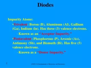
n-type material is formed by adding pentavalent (5 valence electrons) impurity atoms
electrons are called majority carriers in n-type material
holes are called minority carriers in n-type material
p-type material is formed by adding trivalent (3 valence electrons) impurity atoms
holes are called majority carriers in p-type material
electrons are called minority carriers in p-type material
8. The PN Junction Diode A diode consists of an n region and a p region separated by a pn junction
the n region has many conduction electrons
the p region has many holes
As a result of recombination, a large number of positive (in the n region) and negative (in the p region) ions builds up near the pn junction, essentially depleting the region of any conduction electrons or holes - termed the depletion region
9. The PN Junction Diode The barrier potential, VB, is the amount of voltage required to move electrons through the electric field
At 25�C, it is approximately 0.7 V for silicon and 0.3 V for germanium
As the junction temperature increases, the barrier potential decreases, and vice versa
10. The PN Junction Diode Forward bias is the condition that permits current through a diode
the negative terminal of the VBIAS source is connected to the n region, and the positive terminal is connected to the p region
11. The PN Junction Diode The negative terminal of the bias-voltage source pushes the conduction-band electrons in the n region toward the pn junction, while the positive terminal pushes the holes in the p region toward the pn junction
When it overcomes the barrier potential (VB), the external voltage source provides the n region electrons with enough energy to penetrate the depletion region and move through the junction
12. The PN Junction Diode Reverse bias is the condition that prevent current through the diode
the negative terminal of the VBIAS source is connected to the p region, and the positive terminal is connected to the n region
If the external reverse-bias voltage is increased to a large enough value, reverse breakdown occurs
minority conduction-band electrons acquire enough energy from the external source to accelerate toward the positive end of the diode, colliding with atoms and knocking valence electrons into the conduction band
13. Diode Characteristics
14. Diode Characteristics The �arrowhead� in the diode symbol points in the direction opposite the electron flow
The anode (A) is the p region
The cathode (K) is the n region
15. Diode Characteristics The simplest way to visualize diode operation is to think of it as a switch
When forward-biased, the diode ideally acts as a closed (on) switch
When reverse-biased, it acts as an open (off) switch
16. Diode Rectifiers A diode is connected to an ac source that provides the input voltage, Vin, and to a load resistor, RL, forming a half-wave rectifier
on the positive half-cycle, the diode is forward biased
17. Diode Rectifiers When the diode barrier potential is taken into account, as in the practical model, the input voltage must overcome the barrier potential before the diode becomes forward-biased
This results in a half-wave output voltage with a peak value that is 0.7 V less than the peak value of the input voltage
It is often practical to neglect the effect of barrier potential when the peak value of the applied voltage is much greater than the barrier potential
18. Diode Rectifiers Peak Inverse Voltage (PIV) is the maximum value of reverse voltage that a diode can withstand
A full-wave rectifier allows unidirectional current to the load during the entire input cycle
whereas the half-wave rectifier allows this only during one-half of the cycle
The average value for a full-wave rectifier output voltage is twice that of the half-wave rectifier
VAVG = 2VP(out) / ?
19. Diode Rectifiers The full-wave bridge rectifier uses four diodes, as shown on the next slide
When the input cycle is positive as in part (a), diodes D1 and D2 are forward-biased and conduct current, while diodes D3 and D4 are reverse-biased
When the input cycle is negative as in part (b), diodes D3 and D4 are forward-biased and conduct current, while diodes D1 and D2 are reverse-biased
20. Diode Rectifiers
21. Diode Rectifiers Two diodes are always in series with the load during both the positive and negative half-cycles
Neglecting the barrier potentials of the the two diodes, the output voltage is a full-wave rectified voltage with a peak value equal to the peak secondary voltage
The PIV of the diodes must equal the peak secondary voltage:
PIV = VP(out)
22. Power Supplies The dc power supply converts the standard 110 V, 60 Hz ac available at the wall outlets into a constant dc voltage
dc voltage is used in most electronic circuits
A capacitor is used to filter the output of the rectifier, charging during each quarter-cycle that the input voltage exceeds the capacitor voltage, and discharging through the load when the input voltage decreases below the capacitor voltage, at which point the diodes become reverse biased
23. Power Supplies Since the capacitor charges to a peak value equal to VP(in), the peak inverse voltage of the diode in this application must be:
PIV = 2 VP(in)
Ripple voltage is the variation in output voltage due to charging and discharging of the capacitor
For a given input frequency, ripple voltage for a full-wave rectifier will be less than that for a half-wave rectifier
24. Power Supplies An integrated circuit regulator (three-terminal regulator) is a device that is connected to the output of a filtered rectifier and maintains a constant output voltage despite changes in the input voltage or the load current
25. Special Purpose Diodes The zener diode is used to provide an output reference voltage that is stable despite changes in input voltage
Used as a reference in regulated power supplies
The zener diode is designed for operation in the reverse breakdown region, where the voltage remains almost constant over a wide range of reverse current values
26. Special Purpose Diodes A varactor diode utilize the inherent capacitance of the depletion region of a reverse-biased pn junction to vary capacitance by changing the reverse voltage
The p and n regions are conductive, and act as the capacitor plates
The depletion layer created by the reverse bias acts as a capacitor dielectric because it is nonconductive
as the reverse bias increases, the depletion region widens, and the capacitance across the diode decreases
as the reverse bias decreases, the depletion region narrows, and the capacitance across the diode increases
27. Special Purpose Diodes The light-emitting diode (LED)
when the device is forward-biased, electrons cross the pn junction from the n-type material and recombine with holes in the p-type material
Since the electrons in the conduction band are at a higher energy level than the holes in the valence band, when recombination takes place, energy is released in the form of heat and light
A large exposed surface on one layer of the LED permits the photons to be emitted as light, termed electroluminescence
28. Summary The process of adding impurities to an intrinsic (pure) semiconductor to increase and control conductivity is called doping
A p-type semiconductor is doped with trivalent impurity atoms
a n-type semiconductor is doped with pentavalent impurity atoms
The depletion region is a region adjacent to the pn junction containing no majority carriers
29. Summary Forward bias permits majority carrier current through the diode
Reverse bias prevents majority carrier current
The single diode in a half-wave rectifier conducts for half of the input cycle
The PIV is the maximum voltage appearing across the diode in reverse bias
The output frequency of a full-wave rectifier is twice the input frequency
30. Summary A capacitor-input filter provides a dc output approximately equal to the peak of the input
Ripple voltage is caused by the charging and discharging of the filter capacitor
Regulation of output voltage over a range of input voltages is called input or line regulation
The zener diode operates in reverse breakdown
A zener diode maintains an essentially constant voltage across its terminals over a specified range of zener currents
31. Summary Zener diodes can be used as voltage references in a variety of applications
A varactor diode acts as a variable capacitor under reverse-biased conditions
The capacitance of a varactor diode varies inversely with reverse-biased voltage