Diodes
Diodes. Impurity Atoms: Trivalent : Boron (B), Aluminum (Al), Gallium (Ga), Indium (ln). Has three (3) valence electrons. Known as an “Acceptor Impurity.” Pentavalent : Phosphorous (P), Arsenic (As), Antimony (Sb), and Bismuth (Bi). Has five (5) valence electrons.

Diodes
E N D
Presentation Transcript
Diodes • Impurity Atoms: • Trivalent: Boron (B), Aluminum (Al), Gallium (Ga), Indium (ln). Has three (3) valence electrons. • Known as an “Acceptor Impurity.” • Pentavalent: Phosphorous (P), Arsenic (As), Antimony (Sb), and Bismuth (Bi). Has five (5) valence electrons. • Known as a “Donor Impurity.” CENT-112 Fundamentals of Electricity and Electronics
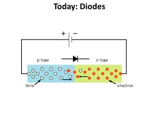
PN Material • “N - Type” Material: • Pure base material doped with a Donor Impurity. • Majority Current Carrier: Electrons • Minority Current Carrier: Holes • “P - Type” Material: • Pure base material doped with an Acceptor Impurity. • Majority Current Carrier: Holes • Minority Current Carrier: Electrons CENT-112 Fundamentals of Electricity and Electronics
Construction • Old Method: Grown Crystals. • Newer Methods: • Alloy Fused: N & P material made using heat / pressure. • Diffused: N & P gas and heat. • Both methods are used to produce a “PN” Junction. CENT-112 Fundamentals of Electricity and Electronics
Questions Q) What is meant by a donor impurity? A) 5 valiant electrons in outer shell. Q) What are 4 examples of a donor impurity? A) Phosphorous, Arsenic, Antimony and Bismuth. CENT-112 Fundamentals of Electricity and Electronics
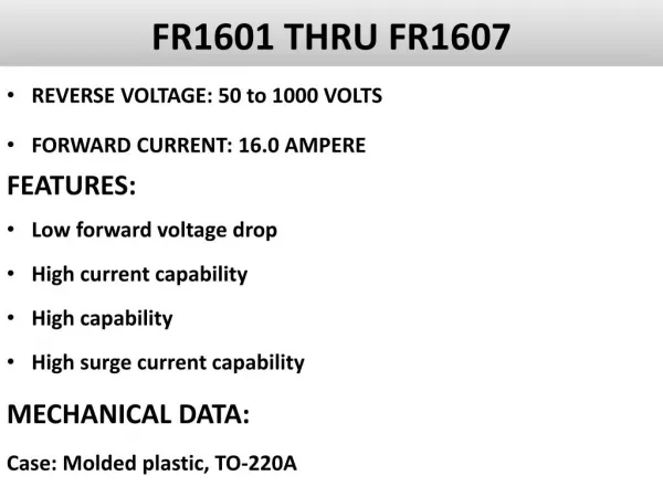
Diode Definitions • Potential Hill (Junction Barrier) : Electrostatic field set up across a PN junction which prevents further combination of majority current carriers. • The value of the voltage of the potential hill depends on the type of base material used during diode construction. • 1. Silicon (.5 - .8V) • 2. Germanium (.2V) • Rated for up to 1500A / 3000V. • Used primarily in Rectifiers. CENT-112 Fundamentals of Electricity and Electronics
Operations & Definitions • Forward Bias: External voltage applied which opposes the potential hill, effectively reducing the width and resistance of the depletion region. => Majority Current Carriers flow through the PN junction. • Reverse Bias: External voltage applied which aids the potential hill, effectively increasing the width and resistance of the depletion region. => No Majority Current Carriers flow through the PN junction. CENT-112 Fundamentals of Electricity and Electronics
Rectifier Diode Block Diagram Depletion Region - - - - N - - - - + + + + P + + + + - - - - - - - - + + + + + + + + Anode Cathode Potential Hill (Junction Barrier) CENT-112 Fundamentals of Electricity and Electronics
Rectifier Diode Schematic Diagram Anode Cathode CENT-112 Fundamentals of Electricity and Electronics
Diode Forward Bias Depletion Region - - - - N - - - - + + + + P + + + + - - - - + + + + Anode Cathode - + Potential Hill (Junction Barrier) CENT-112 Fundamentals of Electricity and Electronics
Diode Reverse Bias Depletion Region - - - - N - - - - + + + + P + + + + - - - - - - - - - - - - + + + + + + + + + + + + Anode Cathode - + Potential Hill (Junction Barrier) CENT-112 Fundamentals of Electricity and Electronics
Characteristic Curve +I (mA) Forward Bias -V a -c +V a -c Reverse Bias -I (uA) Avalanche Breakdown CENT-112 Fundamentals of Electricity and Electronics
Zener Diode • The Zener diode is a heavily doped diode which, as a result of doping, has a very narrow depletion region. This allows the diode to be operated in the reverse biased region of the characteristic curve without damaging the PN junction. • “Zener Effect”: The area of Zener diode operation (<5V) where the Diode maintains a constant voltage output while operating reverse biased. • “Avalanche Effect”:>5V applied to the diode while reverse biased which tends to cause the diode to eventually breakdown due to heat generation within the lattice structure of the crystal. CENT-112 Fundamentals of Electricity and Electronics
Zener Diode Schematic Symbol Anode Cathode CENT-112 Fundamentals of Electricity and Electronics
Characteristic Curve I (mA) Forward Bias Operating Region - V a - c + V a - c Reverse Bias I (uA) CENT-112 Fundamentals of Electricity and Electronics
Zener Operation • Ratings: .25V to 1500V • Used in SSMG / SSTG AC voltage regulator for the reference circuit. • When a higher constant voltage is desired, the zener diodes will be “Stacked” together in series and their voltages will add together to make the higher desired voltage. • This is the case in the SSMG / SSTG AC voltage regulators where four (4) 6v zener diodes are stacked to provide a 24V reference to the comparison circuit. CENT-112 Fundamentals of Electricity and Electronics
Zener Diode Voltage Regulator R1 Vin Vout CR1 CENT-112 Fundamentals of Electricity and Electronics
Signal Diode • Same construction as the Rectifier Diode except that it is designed to operate with a very short “reverse recovery time” to allow it to rectify high frequency AC inputs. CENT-112 Fundamentals of Electricity and Electronics
Power Supplies • Components and their function • Transformer - Receives the AC input from the distribution system and either steps up or down the voltage. • Rectifier - Converts the AC input voltage from the transformer to a pulsating DC voltage. • Filter - Smoothes out the DC pulsations or ripple received from the rectifier. • Regulator - Receives a smoothed DC voltage from the Filter Stage and produces a steady DC voltage to be used by electronic circuitry. CENT-112 Fundamentals of Electricity and Electronics
Half - Wave Rectifier CR1 1 : 1 VIN R1 VOUT T1 CENT-112 Fundamentals of Electricity and Electronics
Half - Wave Rectifier Operation • Positive half-cycle the diode is Forward Bias (FB), negative half-cycle the diode is Reverse Bias (RB). VDC = VPK X .318 Where: VDC = Average DC voltage VPK = Peak input voltage .318 = Constant CENT-112 Fundamentals of Electricity and Electronics
Full - Wave Rectifier CR1 1 : 1 VIN R1 VOUT T1 CR2 CENT-112 Fundamentals of Electricity and Electronics
Full - Wave Rectifier Operation • Positive half-cycle, 1 diode is FB, negative half-cycle the other diode is FB. VDC = VPK X .637 Where: VDC = Average DC voltage VPK = Peak input voltage .637 = Constant CENT-112 Fundamentals of Electricity and Electronics
Full – Wave Bridge Rectifier 1 : 1 CR2 CR1 CR4 CR3 T1 R1 VIN VOUT CENT-112 Fundamentals of Electricity and Electronics
Full - Wave Bridge Rectifier Operation • Positive half-cycle, 1 diode is FB, negative half-cycle the other diode is FB. VDC = VPK X .637 Where: VDC = Average DC voltage VPK = Peak input voltage .637 = Constant CENT-112 Fundamentals of Electricity and Electronics
Filters • A filter uses the characteristics of Inductors and Capacitors to smooth the pulsating DC waveform supplied by the Rectifier. • Types • High Pass - A series RC filter whose output is taken from the resistor. • Series / Parallel - A filter configuration which uses combinations of capacitors and inductors to smooth the voltage and current pulsations from the rectifier output. CENT-112 Fundamentals of Electricity and Electronics
Ideal filter characteristics • Rapid charge time constant for filter capacitors and inductors. • Slow discharge time constant for filter capacitors and inductors. CENT-112 Fundamentals of Electricity and Electronics
Capacitor Filter Configuration • Capacitor Input Filter Schematic Diagram C1 VIN VOUT RB CENT-112 Fundamentals of Electricity and Electronics
Capacitor Filter Operation • Charge RC time constant is developed from the internal resistance of the rectifier diodes and the capacitance of the filter capacitor. The net result is that the low resistance of the rectifier diodes develop a rapid charge RC time constant. • Discharge RC time constant is developed from the filter capacitor and the load resistance. Since the load resistance is rather large, the discharge RC time constant is somewhat long. • RB is called the “Bleeder Resistor” because it provides a path for the filter capacitor(s) to discharge when power is removed from the circuit. RB has a very large resistance and usually draws <10% of normal operating current. CENT-112 Fundamentals of Electricity and Electronics
LC Choke Filter Configuration • LC Choke Filter Schematic Diagram L1 VIN VOUT C1 RB CENT-112 Fundamentals of Electricity and Electronics
LC Choke Filter Operation • Charge RC time constant is developed from the internal resistance of the rectifier diodes, the Low DC resistance of the inductor (L1), and the capacitance of the filter capacitor. The net result is that the low resistance of the rectifier diodes and inductor (L1) develop a rapid charge RC time constant. • Discharge RC time constant is developed from the filter capacitor and the load resistance. Since the load resistance is rather large, the discharge RC time constant is somewhat long. • The Inductor acts to smooth out the current pulsations produced by the rectifier and / or transformer stage of the power supply. CENT-112 Fundamentals of Electricity and Electronics
RC PI Filter Configuration • RC PI Filter Schematic Diagram Charge Path DischargePath R1 VIN VOUT C1 C2 RB VOUT (C2) VOUT(C1) CENT-112 Fundamentals of Electricity and Electronics
RC PI Filter Operation • First Capacitor provides most of the filtering action. • Second Capacitor Provides additional voltage filtering. • Resistor limits current flow to the desired value and establishes the RC time constants for both filter capacitors. CENT-112 Fundamentals of Electricity and Electronics
LC PI Filter Configuration • LC PI Filter Schematic Diagram Charge Path DischargePath L1 VIN C1 C2 RB VOUT (C2) VOUT(C1) CENT-112 Fundamentals of Electricity and Electronics
LC PI Filter Operation • First Capacitor provides most of the filtering action. • Second Capacitor Provides additional voltage filtering. • Inductor opposes changes in current flow to reduce current spikes and establishes the RC time constants for both filter capacitors. CENT-112 Fundamentals of Electricity and Electronics
Voltage Regulators • Series Regulator • Acts as a variable resistor in series with the load. • Zener Diode Voltage Regulator • Schematic R1 Vin Vout CR1 CENT-112 Fundamentals of Electricity and Electronics
Voltage Regulator Operation Vin Vout R1 CR1 VOUT VIN CENT-112 Fundamentals of Electricity and Electronics
Transistor Voltage Regulators Vin Vout CENT-112 Fundamentals of Electricity and Electronics
OPAMP Voltage Regulators - + Vin Vout CENT-112 Fundamentals of Electricity and Electronics