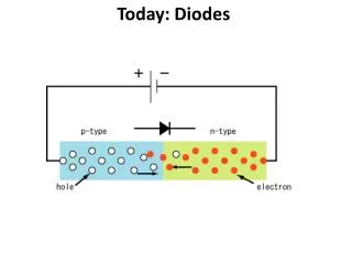
Diodes
Diodes. The simplest and most fundamental nonlinear circuit element. 1. 3.1 The ideal Diode. 3.1.1 Current-Voltage characteristic. (a) diode circuit symbol. (b) i– v characteristic;.


Diodes
E N D
Presentation Transcript
Diodes The simplest and most fundamental nonlinear circuit element Microelectronic Circuits - Fifth Edition Sedra/Smith 1
3.1 The ideal Diode 3.1.1 Current-Voltage characteristic (a) diode circuit symbol (b)i–vcharacteristic; Figure 3.2 The two modes of operation of ideal diodes and the use of an external circuit to limit the forward current (a) and the reverse voltage (b). (c) equivalent circuit in the reverse direction; (d) equivalent circuit in the forward direction. Microelectronic Circuits - Fifth Edition Sedra/Smith
3.1.2 A simple application: Rectifier EXAMPLE3.1 Figure 3.3 (a) Rectifier circuit. (b) Input waveform. 12 V (c) Equivalent circuit when vI 0. (d) Equivalent circuit when vI< 0. (a) Find the fraction of each cycle during which the diode conduct. (b) Find the peak value of the diode current. (c) Find the maximum reverse-bias voltage that appears across the diode. Sol) (a) (b) (e) Output waveform. (c) Microelectronic Circuits - Fifth Edition Sedra/Smith
3.1.3 Diode Logic Gate Find Iand V. Sol) We don’t know whether none, one, or both diodes are conducting. Y=A∙B∙C Make a plausible assumption, proceed with the analysis, and then check whether we end up with a consistent solution ! (a) Assume that both diodes are conducting. VB = 0, V = 0 Y=A+B+C Writing a node equation at B, (a) OR gate (b) AND gate (in a positive-logic system). (b) Assume that both diodes are conducting. EXAMPLE3.2 VB = 0, V = 0 Writing a node equation at B, Impossible !! Assume that D1 is off, and D2 is on. Microelectronic Circuits - Fifth Edition Sedra/Smith
3.2 Terminal Characteristics of Junction Diodes We study the characteristics of real diode - specifically, semiconductor junction diode made of silicon. Figure 3.7 The i–vcharacteristic of a silicon junction diode. Figure 3.8 The diode i–v relationship with some scales expanded and others compressed in order to reveal details. * The characteristic curve consists of three distinct regions: 1. The forward-bias region, determined by υ> 0 2. The reverse-bias region, determined by υ< 0 3. The breakdown region, determined by υ< -VZR Microelectronic Circuits - Fifth Edition Sedra/Smith
3.2.1 The Forward-Bias Region 1. The forward-bias region, determined by υ> 0 This equation can be derived from semiconductor theory. Is = saturation current at a given temperature scale current proportional to the cross-sectional area of the diode order of 10-15 A for low-power small-signal diode very strong function of temperature (doubles for every 5 oC rise) VT = kT/q = thermal voltage υ> 0 k = Boltzmann’s constant =1.38 x 10⁻²³ joules/kelvin T = the absolute temperature in kelvins =273 + temperature in oC q = the magnitude of electronic charge = 1.60 x 10⁻¹⁹ coulomb 25 mV at 20 oC n = 1~2 depending on the material and the physical structure of the diode. 1 for diode made using the standard integrated-circuit fabrication process. (obtained by connecting collector and base, Cha. 5) 2 for discrete diode Microelectronic Circuits - Fifth Edition Sedra/Smith
Threshold voltage υ>0.7 V, fully conducting Cut-in voltage 2.3nVT = 60 mV for n=1, 120 mV for n = 2. Not knowing the exact value of n (which can be obtained from a simple experiment), circuit designers use the convenient approximate number of 0.1 V/decade for the slope of the diode logarithmic characteristic. * Threshold Voltage = Voltage drop: 0.7 V @1 mA for small signal diode, 0.7 V@1 A for high power diode. EXAMPLE3.3 For small signal diode, evaluate ISin the event that n is 1 or 2. Figure 3.9 Illustrating the temperature dependence of the diode forward characteristic. At a constant current, the voltage drop decreases by approximately 2 mV for every 1C increase in temperature. The value of n used can be quite important !!! Microelectronic Circuits - Fifth Edition Sedra/Smith
3.2.2 The Reverse-Bias Region 2. The reverse-bias region, determined by υ< 0 If υis negative and a few times greater than VT (25 mV), Real Diode Reverse current i >> Saturation current I order of 1 nA order of 10-14~10-15. constant increases with reverse voltage diffusion mostly due to leakage doubles for every 5 oC rise doubles for every 10 oC rise 3.2.3 The Breakdown Region 3. The breakdown region, determined by υ< -VZR * VZR : The breakdown voltage, knee voltage, Z stands for zener. * Diode breakdown is normally not destructive provided that the power dissipated in the diode is limited by external circuitry to a safe value specified in data sheets. * Voltage regulation is possible in this region. (Sect. 3.5) Microelectronic Circuits - Fifth Edition Sedra/Smith
3.3 Modeling the diode Forward Characteristic (Detailed analysis of circuits employing diodes) ID=? VD=? Exponential model. Ideal-Diode model Piecewise–Linear model Constant-Voltage-Drop model Small-Signal model 3.3.1 The Exponential Model – the most accurate description of the diode, but difficult to use How to solve this simultaneous equations ? 3.3.2 Graphical Analysis Use the i-υ curve given in the data sheet, ruler, and your eyes. 3.3.3 Iterative Analysis Use computer, but you need programming.-ex. 3.4 Microelectronic Circuits - Fifth Edition Sedra/Smith
thepiecewise-linear model. the constant-voltage-drop model 3.3.4 Theneed for Rapid Analysis * In design process, rapid circuit analysis is necessary, not in the final conformation process. * In the final conformation process, SPICE is the best choice. 3.3.5 The Piecewise-Linear model 3.3.6 The Constant-Voltage-Drop model Microelectronic Circuits - Fifth Edition Sedra/Smith
3.3.7 TheIdeal –Diode Model * This model can be used when input voltage is much greater than the diode voltage drop (0.6~0.8 V). * We have learned this Sect. 3.1. * Useful in determining which diodes are on or off. 3.3.8 TheSmall-signal Model Quiescent point Valid forυd < 10 mV n=2 υd < 5 mV n=1 Diode small-signal conductance (Siemens) Microelectronic Circuits - Fifth Edition Sedra/Smith
n = 2 EXAMPLE3.6 V+= 10 Vdc on which is superimposed υs = 60 Hz sinusoid of 1 V peak (power supply ripple). R = 10 kΩ Calculate both the dc voltage of the diode and the amplitude of the signal appearing on it. Assume the diode to have 0.7 V drop at 1 mA and n = 2. Sol) First, consider dc component only, 0.93 mA ≈1 mA, assumed 0.7 V is valid ! 3.3.9 Use of the Diode Forward Drop in Voltage Regulation Voltage regulator: A circuit keeping its output voltage as constant as possible in spite of; (a) changes in the load current drawn from the regulator output, (b) changes in the dc power supply voltage that feed the regulator. EXAMPLE3.7 (a) Find the % changes in υO caused by a ±10 % change in the dc power supply voltage. (b) Find the % changes in υO caused by connection of 1 kΩ load resistance. Microelectronic Circuits - Fifth Edition Sedra/Smith
3.4 Operation in the Reverse Breakdown Region-Zener Diodes Voltage regulators are operating in this region. Special diodes that are manufactured to operate in the breakdown region are called breakdown diodes or zener diodes. 3.3.9 Specifying and Modeling the Zener Diodes IZK : knee current (data sheet) VZ : voltage across the diode at the test current IZT (data sheet) a few volts ~ a few hundred volts. rZ : incremental (dynamic) resistance at Q (data sheet) a few~ a few tens of ohms. 0.5 W (data sheet), 6.8 V can operates safely at 70 mA, maximum. Microelectronic Circuits - Fifth Edition Sedra/Smith
EXAMPLE3.8 VZ = 6.8 V @ Iz = 5 mA, rz=20Ω, IZK = 0.2 mA (a) VO =? w/o load and w/ V+ at its nominal value. IL≈ 6.8 V/2 kΩ=3.4 mA (b) ∆VO =? w/ ±1 V change in V+. ∆VO/ ∆V+( mV/V) is known as line regulation. For more rigorous calculation, you have to analyze the circuit in Fig. (b). 70 mA (e) VO =? w/ RL = 0.5 kΩ 6.8 V/ 0.5 kΩ = 13.6 mA. Is this possible ? Impossible!! Maximum I through R = 6.4 mA!! The zener diode operates in reverse-bias region !! (c) ∆ VO =? w/ RL (IL = 1mA). Find load regulation ∆VO/ ∆IL( mV/mA). The zener diode is off (open circuit). When a load resistance RL is connected that draws a current IL = 1mA, the zener current will decrease by 1 mA. (e) Minimum RL for break down region = ? Iz = IZK = 0.2 mA at the edge of the breakdown region, The lowest (worst-case) current through R = (9-6.7)/0.5 = 4.6 mA), then the load current = 4.6 - 0.2 = 4.4 mA (d) ∆ VO =? w/ RL = 2 kΩ Microelectronic Circuits - Fifth Edition Sedra/Smith
Power transformer The dc voltage VO is required to be as constant as possible in spite of variations in the ac line voltage and in the current drawn by the load. 3.5 Rectifier Circuit – one of the most important applications of diodes- dc power supplies Power transformer : 1. V2=(N2/N1)V1 2. Electrical isolation between the electronic devices and the power-line circuit. This isolation minimizes the risk of electric shock to the equipment user. Diode rectifier : convert the input sinusoid υSto a unipolar output. Filter : reducing the variations in the magnitude of the rectifier output. Voltage regulator : 1.reducing ripple 2. Stabilizing the magnitude of the dc output voltage of the supply against variations caused by changes in load current. 3. Circuit using zener diode or IC regulator (7805, 7915) Microelectronic Circuits - Fifth Edition Sedra/Smith
3.5.1 The Half-Wave Rectifier. Microelectronic Circuits - Fifth Edition Sedra/Smith
3.5.2 The Full-Wave Rectifier. Microelectronic Circuits - Fifth Edition Sedra/Smith
3.5.3 The Bridge Rectifier. Microelectronic Circuits - Fifth Edition Sedra/Smith
3.5.4 The Rectifier with a Filter Capacitor - The Peak Rectifier Vr =? ∆t =? iDav =? during conduction time For C, Qsupplied during on time=Qlost during off time iCav= iDav - IL Qsupplied =iCav∆t, Qlost =CVr Microelectronic Circuits - Fifth Edition Sedra/Smith
EXAMPLE3.9 Design specification Input: 60 Hz, sinusoid Output: Vp=100 V, peak-to-peak ripple 2 V Load: 10 kΩ C=? 0.2/(2*3.14)=3.18% Diode on-time/cycle =? Average diode current =? Peak diode current =? Figure 3.30 Waveforms in the full-wave peak rectifier. * Comparing with the half-wave case, we need half size capacitor, half diode currents. The most important design parameters !! This peak-rectifier can be applied to the design of a peak detector and a demodulator for a amplitude–modulated (AM) signals. Microelectronic Circuits - Fifth Edition Sedra/Smith
3.5.5 Precision Half-wave Rectifier-the Super Diode We need a very high-performance rectifier circuit that has no voltage drop (0.7 V) in some applications !! 1. Initially, υI= υO=0 5. When υI≈ 0<0, υA≈A υI<< 0 V 6. Diode is off. 2. When υI≈ 0>0, υA≈A υI>>0.7 V 3. Diode conducts 7. Open loop ! υAwill saturate. 4. Voltage follower ! Unity gain amplifier ! Buffer amplifier ! 8. υO= 0 V Microelectronic Circuits - Fifth Edition Sedra/Smith
3.6 Limiting and Clamping Circuits 3.6.1 Limiter Circuits Double limiter Microelectronic Circuits - Fifth Edition Sedra/Smith
RC LPF demodulator 3.6.2 TheClamped Capacitor or DC Restorer The clamped capacitor or dc restorer with a square-wave input and no load. Peak rectifier * The output waveform will have its lowest peak clamped to 0 V. * Reversing diode polarity will provide an output waveform whose highest peak is clamped to 0 V. Pulse width modulation (PWM) DC Restorer ! Microelectronic Circuits - Fifth Edition Sedra/Smith
3.6.3 TheVoltage Doubler or Multiplier This technique can be extended to provide dc output voltage that are higher multiples of Vp. Microelectronic Circuits - Fifth Edition Sedra/Smith
3.7 Physical Operation of Diodes 3.7.1 Basic Semiconductor Concepts • Electronic materials fall into three categories: J (A/m2)= σE(V/m),ρ(A-m/V)=1/σ • Insulators Resistivity () > 105-cm • Semiconductors 10-3 < < 105 -cm • Conductors < 10-3 -cm • Elemental semiconductors are formed from a single type of atom (IV, Si, Ge) • Compound semiconductors are formed from combinations of column III and V elements or columns II and VI. • Germanium was used in many early devices. • Silicon quickly replaced silicon due to its higher bandgap energy, lower cost, and is easily oxidized to form silicon-dioxide insulating layers. Microelectronic Circuits - Fifth Edition Sedra/Smith
Silicon Covalent Bond Model (cont.) Increasing temperature adds energy to the system and breaks bonds in the lattice, generating electron-hole pairs. Near absolute zero, all bonds are complete. Each Si atom contributes one electron to each of the four bond pairs. n =p= ni. ni=concentration of carriers in intrinsic semiconductor Microelectronic Circuits - Fifth Edition Sedra/Smith
Intrinsic Carrier Concentration • The density of carriers in a semiconductor as a function of temperature and material properties is: • EG = semiconductor bandgap energy in eV (electron volts) • k = Boltzmann’s constant, 8.62 x 10⁻⁵ eV/K • T = absolute termperature, K • B = material-dependent parameter, 1.08 x 1031 K-3 cm-6 for Si • Bandgap energy is the minimum energy needed to free an electron by breaking a covalent bond in the semiconductor crystal. • ni2 ≈ 1.5x1010 cm-3 for Si at 300 K (room temperature) Diffusion current and Drift current Diffusion current • Dp and Dn are the hole and electron diffusivities with units cm2/s. Microelectronic Circuits - Fifth Edition Sedra/Smith
Diffusivity and mobility are related by Einstein’s relationship: Drift current Doped Semiconductor • Doping is the process of adding very small well controlled amounts of impurities into a semiconductor. • Doping enables the control of the resistivity and other properties over a wide range of values. • For silicon, impurities are from columns III and V of the periodic table. Microelectronic Circuits - Fifth Edition Sedra/Smith
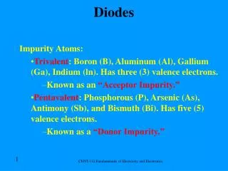
Acceptor Impurities in Silicon Donor Impurities in Silicon • Boron (column III element) has been added to silicon. • There is now an incomplete bond pair, creating a vacancy for an electron. • Little energy is required to move a nearby electron into the vacancy. • As the ‘hole’ propagates, charge is moved across the silicon. • p type! • Phosphorous (or other column V element) atom replaces silicon atom in crystal lattice. • Since phosphorous has five outer shell electrons, there is now an ‘extra’ electron in the structure. Free electron! • Material is still charge neutral, but very little energy is required to free the electron for conduction since it is not participating in a bond. • n type ! In thermal equilibrium, concentration of donor atoms = concentration of free electrons Free electrons (holes) in n-type silicon are majority carriers and holes (free electrons) in p-type silicon are minority carriers. Thermally generated hole is decreased. Therefore, A piece of n-type or p-type silicon is electrically neutral !! Microelectronic Circuits - Fifth Edition Sedra/Smith
Minority carriers 3.7.2 The pn junction Under Open-Circuit Conditions E field Diffusion current! Diffusion Acceptors (B, III) accept, recombine with electrons and become (-). Donors (P, IV) donate electrons and become (+). Drift current! This process produces electric potential and field and stops when coulomb force equals to diffusion mechanism. E field 0.1~1 μm There is no free electron and holes in this region. This region is depleted of free carriers !! 0.6~0.8 V Microelectronic Circuits - Fifth Edition Sedra/Smith
3.7.3 The pn junction Under Reverse-Bias Conditions Figure 3.46 The pn junction excited by a constant-current source I in the reverse direction. To avoid breakdown, I is kept smaller than IS.Note that the depletion layer widens and the barrier voltage increases by VRvolts, which appears between the terminals as a reverse voltage. m : grading coefficient depends on the concentration profile. Microelectronic Circuits - Fifth Edition Sedra/Smith
3.7.5 The pn junction Under Forward-Bias Conditions Figure 3.50Minority-carrier distribution in a forward-biased pn junction. It is assumed that the p region is more heavily doped than the n region; NA >>ND. Lp diffusion length 1~100 μm τp : excess-minority-carrier-lifetime Microelectronic Circuits - Fifth Edition Sedra/Smith
Diffusion capacitance τT : mean transit time Junction (depletion-layer) capacitance But accuracy is poor. Microelectronic Circuits - Fifth Edition Sedra/Smith
3.8 Special Diode Types 3.8.1 The Schottky-(Barrier) Diode (SBD) - Metal (anode)-moderately doped n-type semiconductor (cathode) junction. - Current is conduced by majority carriers (electrons). No minority-carrier charge-storage effect Much faster on-off transit time! - 0.3 ~0.5 V forward voltage drop. GaAs SBD (very fast) voltage drop: ~0.7 V - Not every metal-semiconductor contact is a diode. - Ohmic contact for diode lead is metal-heavily doped semiconductor juction. 3.8.2 Varactors - Special diode that are fabricated to be used as voltage-variable capacitor. - Cj is made to be strong function of reverse voltage (m = 3~4) - These are used for automatic tuning of radio receivers. 3.8.3 Photodiodes - Special diode that can be used to convert light power to electric current. - A photon that has energy greater than the band-gap energy generate electron-hole pair. - This electron-hole pair cause the current to flow through the reversely biased diode. - The photodiode is an important component of a growing family of circuits known as optoelectronics or photonics. - Fiber-optic communication, CD-ROM, automatic door, automatic flusher…(phototransistors) - The photodiode without reverse bias is a solar cell (silicon). - The photodiodes are made of silicon or compound semiconductor (III and V, such as GaAs, InAlGaAs…) Microelectronic Circuits - Fifth Edition Sedra/Smith
3.8.4 Light-Emitting Diodes (LED) and Laser Diodes (LD) - LED converts a forward current into light. - Diffusing minority carriers recombine with majority carriers resulting in emission of photons with energy equal to bandgap energy. - This can be done by fabricating the pn junction using a semiconductor of the type known as direct bandgap materials such as GaAs. - Diffusing minority carriers recombine with majority carriers resulting in emission of photons with energy equal to bandgap energy. - LED display, light source in optical communications (LAN), illumination,… - Laser diode produces coherent light with a very narrow bandwidth. - Laser diodes are used in optical communication, CD players, pointers, laser machining, medical instruments….. - LED + photodiode or phototransistor = optoisolator : complete electrical isolation between electrical circuit that is connected to the isolator’s input and the circuit that is connected to its output. - Optoisolator reduces the effect of electrical interference, can be used in the design of medical instruments to reduce the risk of electrical shock to patients. Microelectronic Circuits - Fifth Edition Sedra/Smith