Semiconductor Diodes
Chapter 19. Semiconductor Diodes. Introduction Diodes Electrical Properties of Solids Semiconductors pn Junctions Semiconductor Diodes Special-Purpose Diodes Diode Circuits. 19.1. Introduction.

Semiconductor Diodes
E N D
Presentation Transcript
Chapter 19 Semiconductor Diodes • Introduction • Diodes • Electrical Properties of Solids • Semiconductors • pn Junctions • Semiconductor Diodes • Special-Purpose Diodes • Diode Circuits
19.1 Introduction • This course adopts a top-down approach to the subject and so far we have taken a ‘black-box’ view of active components (such as op-amps) • It is now time to look ‘inside the box’ • we will start by looking at diodes and semiconductors • then progress to transistors • later we will look at more detailed aspects of circuit design
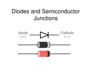
19.2 Diodes • An ideal diode passing electricity in one direction but not the other
One application of diodes is in rectification • the example below shows a half-wave rectifier • In practice, no real diode has ideal characteristics but semiconductor pn junctions make good diodes • To understand such devices we need to look at some properties of materials
19.3 Electrical Properties of Solids • Conductors • e.g. copper or aluminium • have a cloud of free electrons (at all temperatures above absolute zero). If an electric field is applied electrons will flow causing an electric current • Insulators • e.g. polythene • electrons are tightly bound to atoms so few can break free to conduct electricity
Semiconductors • e.g. silicon or germanium • at very low temperatures these have the properties of insulators • as the material warms up some electrons break free and can move about, and it takes on the properties of a conductor - albeit a poor one • however, semiconductors have several properties that make them distinct from conductors and insulators
19.4 Semiconductors • Pure semiconductors • thermal vibration results in some bonds being broken generating free electrons which move about • these leave behind holes which accept electrons from adjacent atoms and therefore also move about • electrons are negative charge carriers • holes are positive charge carriers • At room temperatures there are few charge carriers • pure semiconductors are poor conductors • this is intrinsic conduction
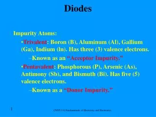
Doping • the addition of small amounts of impurities drastically affects its properties • some materials form an excess of electrons and produce an n-type semiconductor • some materials form an excess of holes and produce a p-type semiconductor • both n-type and p-type materials have much greater conductivity than pure semiconductors • this is extrinsic conduction
The dominant charge carriers in a doped semiconductor (e.g. electrons in n-type material) are called majority charge carriers. Other type are minority charge carriers • The overall doped material is electrically neutral
19.5 pn Junctions • When p-type and n-type materials are joined this forms a pn junction • majority charge carriers on each side diffuse across the junction where they combine with (and remove) charge carriers of the opposite polarity • hence around the junction there are few free charge carriers and we have a depletion layer (also called a space-charge layer)
The diffusion of positive charge in one direction and negative charge in the other produces a charge imbalance • this results in a potential barrier across the junction
Potential barrier • the barrier opposes the flow of majority charge carriers and only a small number have enough energy to surmount it • this generates a small diffusion current • the barrier encourages the flow of minority carriers and any that come close to it will be swept over • this generates a small drift current • for an isolated junction these two currents must balance each other and the net current is zero
Forward bias • if the p-type side is made positive with respect to the n-type side the height of the barrier is reduced • more majority charge carriers have sufficient energy to surmount it • the diffusion current therefore increases while the drift current remains the same • there is thus a net current flow across the junction which increases with the applied voltage
Reverse bias • if the p-type side is made negative with respect to the n-type side the height of the barrier is increased • the number of majority charge carriers that have sufficient energy to surmount it rapidly decreases • the diffusion current therefore vanishes while the drift current remains the same • thus the only current is a small leakage current caused by the (approximately constant) drift current • the leakage current is usually negligible (a few nA)
Forward and reverse currents • pn junction current is given approximately by • where I is the current, e is the electronic charge, V is the applied voltage, k is Boltzmann’s constant, T is the absolute temperature and (Greek letter eta) is a constant in the range 1 to 2 determined by the junction material • for most purposes we can assume = 1
Thus at room temperature e/kT~ 40 V-1 • If V > +0.1 V • If V < -0.1 V • IS is the reverse saturation current
19.6 Semiconductor Diodes • Forward and reverse currents
Silicon diodes • generally have a turn-on voltage of about 0.5 V • generally have a conduction voltage of about 0.7 V • have a breakdown voltage that depends on their construction • perhaps 75 V for a small-signal diode • perhaps 400 V for a power device • have a maximum current that depends on their construction • perhaps 100 mA for a small-signal diode • perhaps many amps for a power device
19.7 Special-Purpose Diodes • Light-emitting diodes • discussed earlier when we looked at light actuators
Zener diodes • uses the relatively constantreverse breakdown voltageto produce a voltagereference • breakdown voltage is calledthe Zener voltage,VZ • output voltage of circuit shown is equal to VZ despitevariations in input voltage V • a resistor is used to limitthe current in the diode
Schottky diodes • formed by the junction between a layer of metal (e.g. aluminium) and a semiconductor • action relies only on majority charge carriers • much faster in operation than a pn junction diode • has a low forward voltage drop of about 0.25 V • used in the design of high-speed logic gates
Tunnel diodes • high doping levels producea very thin depletion layerwhich permits ‘tunnelling’of charge carriers • results in a characteristicwith a negative resistanceregion • used in high-frequency oscillators, where they can be used to ‘cancel out’ resistance in passive components
Varactor diodes • a reversed-biased diode has two conducting regions separated by an insulating depletion region • this structure resembles a capacitor • variations in the reverse-bias voltage change the width of the depletion layer and hence the capacitance • this produces a voltage-dependent capacitor • these are used in applications such as automatic tuning circuits
19.8 Diode Circuits • Half-wave rectifier • peak output voltage is equal to the peak input voltage minus the conduction voltage of the diode • reservoir capacitor used to produce a steadier output
Full-wave rectifier • use of a diodebridge reducesthe time for whichthe capacitor hasto maintain theoutput voltageand thus reducedthe ripple voltage
Signal rectifier • used to demodulatefull amplitudemodulated signals(full-AM) • also known as anenvelope detector • found in a wide rangeof radio receivers fromcrystal sets to superheterodynes
Signal clamping • a simple form ofsignal conditioning • circuits limit theexcursion of thevoltage waveform • can use a combination of signal and Zenerdiodes
Catch diode • used when switchinginductive loads • the large back e.m.f.can cause problemssuch as arcing in switches • catch diodes provide a low impedance path across the inductor to dissipate the stored energy • the applied voltage reverse-biases the diode which therefore has no effect • when the voltage is removed the back e.m.f. forward biases the diode which then conducts
Key Points • Diodes allow current to flow in only one direction • At low temperatures semiconductors act like insulators • At higher temperatures they begin to conduct • Doping of semiconductors leads to the production of p-type and n-type materials • A junction between p-type and n-type semiconductors has the properties of a diode • Silicon semiconductor diodes approximate the behaviour of ideal diodes but have a conduction voltage of about 0.7 V • There are also a wide range of special purpose diodes • Diodes are used in a range of applications