Semiconductor Diodes
Semiconductor Diodes. A diode is a two-terminal device that allows current flow only in one direction.

Semiconductor Diodes
E N D
Presentation Transcript
Semiconductor Diodes • A diode is a two-terminal device that allows current flow only in one direction. • We look in detail at rectifier diodes and Zener diodes. Rectifier circuits convert an a.c. voltage into a ‘pulsating d.c. voltage’. Zener diodes are used to provide a stable voltage reference from a varying supply voltage.
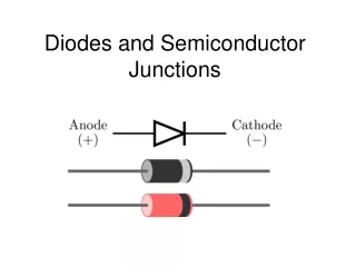
Semiconductor Diodes • The symbols for these two types of diode are (after Smith and Dorf): Rectifier Zener diode
Semiconductor Diodes • The device is a piece of semiconductor material (typically silicon) part of which is doped to be n-type and the other part p-type (One would typically start with an n-type slab and diffuse p-type impurities into part of it at higher concentration to make that region overall p-type. Metal pads are added so metal wires can be attached.)
Semiconductor Diodes • The essential electrical characteristic of a p-n junction is that it constitutes a rectifier • i.e easy current flow in one direction; restrained current flow in the other. • How is this achieved?
Semiconductor Diodes • There is a high concentration of holes on one side of the junction and a high concentration of electrons on the other side. • This causes the two carriers to diffuse to the other side of the junction. (Holes from the p-type region towards the n-type one, electrons the other way)
Semiconductor Diodes • The electrons, which move from the n-type semiconductor to the p-semiconductor, recombine with holes there. • This process leaves fixed negatively charged ions unmatched near the junction on the p-side.
Semiconductor Diodes • Similarly an excess positive charge builds up near the junction in the n-semiconductor. • The 'charging up' exerts a repulsive force on further charges crossing the junction. i.e. a p.d. called the barrier potential difference is produced which opposes the diffusion of charge across the junction. This p.d. will be called Vo. • For a silicon p-n junction Vo 0.6-0.7 Volts
Semiconductor Diodes • The barrier p.d. has a strong electric field associated with it. • This region near the junction is called the depletion region since, to a close approximation, it is free of electron and hole carriers. (Any thermally generated carriers in this transition region would be swept away by the field). • It is noted that a junction capacitance is associated with the depletion layer (It effectively acts like an insulating region between two (semi-)conducting plates)
Semiconductor Diodes • Reverse bias condition • Here an external potential of V volts is applied across the p-n junction with the positive connected to the n region and negative to the p. • The net result is a widening of the depletion region, which establishes too great a potential barrier for majority carriers to overcome. • Majority carrier flow is reduced to zero.
Semiconductor Diodes • Reverse bias condition (continued) • A small reverse saturation current can exist due to thermally generated minority carriers that diffuse towards the junction. (When they get there the junction voltage assists their passage over.) • The reverse saturation currentis given the symbol IO • IOis typically 10-9 A (1 nA) for a silicon junction. • For very large reverse bias the junction can break down causing an abrupt increase in reverse current
Semiconductor Diodes Forward bias • Here an external voltage is applied with the positive to the p-type material and the negative to the n-type material. • The barrier height is reduced from Vo to (Vo - V) (This is because bulk n- and p- regions have lower resistance so most of the applied potential is dropped across the depletion layer).
Semiconductor Diodes Forward bias (Continued) • A large number of majority carriers now have sufficient energy to cross potential barrier. • These majority carriers constitute the dominant component of the forward diode current. • The balance between the tendencies to diffuse and drift is destroyed and ‘diffusion of majority carriers rules’.
Semiconductor Diodes, Summary • In a forward biased diode majority carrier flow dominates. • Hole and electron flow contribute a current in the same direction: i.e. Total current = hole current + electron current. • The relative contribution of electron and holes to the diode current depends on the relative doping of the p- and n- regions. (Important for later discussion of bipolar junction transistors.) • The barrier height cannot become zero because bulk resistance effects in the semiconductor regions limit the current. The bulk p- and n- region resistance is around 1