Logic Gates and Circuits: Fundamentals and Applications
Discover the basics of digital logic circuits, covering logic gates, Boolean algebra, combinational circuits, sequential circuits, and memory components. Learn about various logic gates, basic logic blocks, and the design of logic circuits using truth tables, Boolean functions, and Karnaugh Maps.

Logic Gates and Circuits: Fundamentals and Applications
E N D
Presentation Transcript
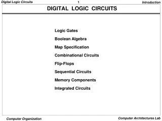
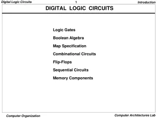
Introduction DIGITAL LOGIC CIRCUITS Logic Gates Boolean Algebra Map Specification Combinational Circuits Flip-Flops Sequential Circuits Memory Components
Logic Gates BASIC LOGIC BLOCK - GATE - Binary Digital Output Signal Binary Digital Input Signal Gate . . . Types of Basic Logic Blocks - Combinational Logic Block Logic Blocks whose output logic value depends only on the input logic values - Sequential Logic Block Logic Blocks whose output logic value depends on the input values and the state (stored information) of the blocks Functions of Gates can be described by - Truth Table - Boolean Function - Karnaugh Map
Logic Gates COMBINATIONAL GATES Name Symbol Function Truth Table A B X A X = A • B X or B X = AB 0 0 0 0 1 0 1 0 0 1 1 1 0 0 0 0 1 1 1 0 1 1 1 1 AND A B X A X X = A + B B OR A X I 0 1 1 0 A X X = A A X 0 0 1 1 Buffer A X X = A A B X A X X = (AB)’ B 0 0 1 0 1 1 1 0 1 1 1 0 NAND A B X A X X = (A + B)’ B 0 0 1 0 1 0 1 0 0 1 1 0 NOR A B X A X = A B X or B X = A’B + AB’ XOR Exclusive OR 0 0 0 0 1 1 1 0 1 1 1 0 A B X A X = (A B)’ X or B X = A’B’+ AB XNOR 0 0 1 0 1 0 1 0 0 1 1 1 Exclusive NOR or Equivalence
Boolean Algebra LOGIC CIRCUIT DESIGN x y z F 0 0 0 0 0 0 1 1 0 1 0 0 0 1 1 0 1 0 0 1 1 0 1 1 1 1 0 1 1 1 1 1 Truth Table Boolean Function F = x + y’z x F y Logic Diagram z
Boolean Algebra BASIC IDENTITIES OF BOOLEAN ALGEBRA [1] x + 0 = x [3] x + 1 = 1 [5] x + x = x [7] x + x’ = 1 [9] x + y = y + x [11] x + (y + z) = (x + y) + z [13] x(y + z) = xy +xz [15] (x + y)’ = x’y’ [17] (x’)’ = x [2] x • 0 = 0 [4] x • 1 = x [6] x • x = x [8] x • X’ = 0 [10] xy = yx [12] x(yz) = (xy)z [14] x + yz = (x + y)(x + z) [16] (xy)’ = x’ + y’ [15] and [16] : De Morgan’s Theorem
Boolean Algebra EQUIVALENT CIRCUITS Many different logic diagrams are possible for a given Function F = ABC + ABC’ + A’C .......…… (1) = AB(C + C’) + A’C [13] ..…. (2) = AB • 1 + A’C [7] = AB + A’C [4] ...…. (3) A B C (1) (2) (3) F A B C F A B C F
Boolean Algebra COMPLEMENT OF FUNCTIONS A,B,...,Z,a,b,...,z A’,B’,...,Z’,a’,b’,...,z’ (p + q) (p + q)’ - Replace all the operators with their respective complementary operators AND OR OR AND - Basically, extensive applications of the DeMorgan’s theorem (x1 + x2 + ... + xn )’ x1’x2’... xn’ (x1x2 ... xn)' x1' + x2' +...+ xn'
Map Simplification SIMPLIFICATION Boolean Function Truth Table Many different expressions exist Unique Karnaugh Map(K-map) is a simple procedure for simplifying Boolean expressions. Truth Table Simplified Boolean Function Karnaugh Map Boolean function
Combinational Logic Circuits x y c s 0 0 0 0 0 1 0 1 1 0 0 1 1 1 1 0 x y c s COMBINATIONAL LOGIC CIRCUITS y y Half Adder 0 0 0 1 1 1 0 x 0 x c = xy s = xy’ + x’y = x y Full Adder y y x y cn-1 cn s 0 1 0 0 0 0 0 0 0 0 0 1 0 1 0 1 0 0 1 0 1 1 1 0 1 0 0 0 1 1 0 1 1 0 1 1 0 1 0 1 1 1 1 1 1 0 0 1 cn-1 cn-1 0 1 1 1 x x 0 0 1 1 cn s cn = xy + xcn-1+ ycn-1 = xy + (x y)cn-1 s = x’y’cn-1+x’yc’n-1+xy’c’n-1+xycn-1 = x y cn-1 = (x y) cn-1 x y S cn cn-1
Combinational Logic Circuits COMBINATIONAL LOGIC CIRCUITS Other Combinational Circuits Multiplexer Encoder Decoder etc
Combinational Logic Circuits Select Output S1 S0 Y 0 0 I0 0 1 I1 1 0 I2 1 1 I3 MULTIPLEXER 4-to-1 Multiplexer I0 I1 Y I2 I3 S0 S1
Combinational Logic Circuits D1 A0 D2 A1 D3 D4 D5 A2 D6 E A1 A0 D0 D1 D2 D3 D7 0 0 0 0 1 1 1 0 0 1 1 0 1 1 0 1 0 1 1 0 1 0 1 1 1 1 1 0 1 d d 1 1 1 1 ENCODER/DECODER Octal-to-Binary Encoder 2-to-4 Decoder D0 D1 A0 D2 D3 A1 E
Sequential Circuits SEQUENTIAL CIRCUITS - Registers A0 A1 A2 A3 Q Q Q Q C C C C D D D D Clock I0 I1 I2 I3 Shift Registers Serial Output Serial Input Clock D Q C D Q C D Q C D Q C Bidirectional Shift Register with Parallel Load A3 A1 A0 A2 Q Q Q Q C C C C D D D D 4 x 1 MUX 4 x 1 MUX 4 x 1 MUX 4 x 1 MUX Serial Input I3 I0 Clock S0S1 I1 I2 SeriaI Input
Memory Components n data input lines k address lines Read Write 2k Words (n bits/word) n data output lines MEMORY COMPONENTS 0 Logical Organization words (byte, or n bytes) N - 1 Random Access Memory - Each word has a unique address - Access to a word requires the same time independent of the location of the word - Organization
Memory Components READ ONLY MEMORY(ROM) Characteristics - Perform read operation only, write operation is not possible - Information stored in a ROM is made permanent during production, and cannot be changed
Question • The following memory units are specified by the number of words times the number of bits per word. How many address lines and input-output data lines are needed in each case? • (a)2K x 16. • (b)64M x 8. • (c)16G x 32.
Question • Specify the number of bytes that can be stored in the memories listed in he following memory units: • (a)2K x 16. • (b)64M x 8. • (c)16G x 32.
REPRESENTATION OF NUMBERS Decimal Binary Octal Hexadecimal 00 0000 00 0 01 0001 01 1 02 0010 02 2 03 0011 03 3 04 0100 04 4 05 0101 05 5 06 0110 06 6 07 0111 07 7 08 1000 10 8 09 1001 11 9 10 1010 12 A 11 1011 13 B 12 1100 14 C 13 1101 15 D 14 1110 16 E 15 1111 17 F Binary, octal, and hexadecimal conversion Octal 1 2 7 5 4 3 Binary 1 0 1 0 1 1 1 1 0 1 1 0 0 0 1 1 Hexa
Questions • Convert the following binary numbers to decimal: • 10011100 • 00110110 • Convert the following decimal numbers to binary : • 70 • 160 • Convert the following binary numbers to Hexadecimal: • 1100 1010 0011 • 0110 1000 1100 0000