Download
1 / 12
190 likes | 531 Vues
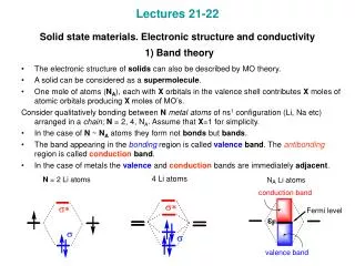
Lectures 21-22 Solid state materials. Electronic structure and conductivity 1) Band theory. The electronic structure of solids can also be described by MO theory. A solid can be considered as a supermolecule .

E N D
Lectures 21-22Solid state materials. Electronic structure and conductivity1) Band theory • The electronic structure of solids can also be described by MO theory. • A solid can be considered as a supermolecule. • One mole of atoms (NA), each with X orbitals in the valence shell contributes X moles of atomic orbitals producing X moles of MO’s. Consider qualitatively bonding between Nmetal atoms of ns1 configuration (Li, Na etc) arranged in a chain; N = 2, 4, NA. Assume that X=1 for simplicity. • In the case of N~NA atoms they form not bonds but bands. • The band appearing in the bonding region is called valenceband. The antibonding region is called conductionband. • In the case of metals the valence and conduction bands are immediately adjacent.
2) Band theory. Insulators, semiconductors, conductors • If we apply now an electrostatic potential to a conductor, the population of the energy levels will tend to change and electrons will be able to flow using empty adjacent conductionband. • In the case of insulators and semiconductors, the energy gap between the valence and conduction bands is more or less significant; electrons cannot easily get into the conduction band and cannot move along the sample; thermal or photo-energy is needed to bring some electrons to the conduction band.
3) Crystal Orbital theory • The band structure of a crystalline material of virtually any complexity can be found through the application of the MO theory for solid state materials (Crystal Orbital theory). • One of the ways to model a real (finite size) crystal is by using cyclic boundary conditions assuming that a chain of bound atoms forms a very large ring. • It turns out that the energy levels in a cyclic molecule composed of N hydrogen atoms look as shown below.
4) Crystal orbitals (Bloch functions) • If we have N hydrogen atoms with atomic wave functions fm (m = 1 … N) related by symmetry and spaced at distance a, we can get N MO’s yn (n = -N/2, …, 0, …, N/2) which are called Bloch functions. • For the n-th crystal orbital, yn, we will have: • When n changes from 0 to N/2, variable k = 2pn/(aN)) (wave vector) changes from 0 to p/a and the type of the MO changes from the completely bondingy0 to the completely antibondingyN/2: • Energy levels of the resulting set of MO’s (band structure) can be described with help of continuous functions E and density of states dn/dE (DOS)
5) Bonding in solids: Crystal Orbital Overlap Population • A common way to analyze bonding in solids is by calculating and analyzing the crystal orbital overlap population (COOP). • COOP is defined in the same way as the bond order is defined in MO theory of molecules. • For any two atoms i and j COOP(i-j) = S2cicjSij (Sij is the overlap integral for two atomic wavefunctions; summation should be performed for all pairs of overlapping orbitals of atoms i and j). A negative value of COOP means antibonding situation while a positive value is characteristic for bonding. • For the chain of hydrogen atoms the lower half of the band is bonding while the upper half is antibonding (see diagram on the right).
6) Simplified picture of bonding in crystalline metals • Using crystal orbital theory we can rationalize the well-known fact that the metals with highest melting points are those belonging to 6th and 7th groups (see diagram below).
7) The Peierls distortion • When working with highly symmetrical structures one has to be cautious. • Highly symmetrical structures with not completely filled degenerate or near-degenerate levels are a subject to distortions which lower the symmetry and the energy of the system (Peierls distortion). • Diagrams on the left and in the center show how we can form bands for polymeric dihydrogen (s-MO) with twice larger four-atomic unit 2a and then distort the polymer to produce an array of dihydrogen molecules (the diagram on the right). • Similarly an infinite polyene -HC=HC-HC=HC-… polyacetylene will have alternating HC-HC and HC=HC bonds due to the Peierls distortion. Because of the large band gap it will behave not as a conductor but as an semiconductor.
8)Band structure of one dimensional polymers: a stack of PtII square planar complexes • In some cases one dimensional consideration is sufficient for a satisfactory analysis of band structure of solids – one dimensional polymers. For example, we can get a satisfactory description of bonding and conductivity of K2[Pt(CN)4Clx] (x = 0 … 0.3) using just one-dimensional model of crystal. • The complexes K2[Pt(CN)4Clx] (x = 0 … 0.3) have Pt(CN)4 – squares stacked one above another with Pt-Pt separation of 3.3 (x = 0) or 2.7-3.3 Ǻ (0 < x < 0.3). • Purely PtII complex (x = 0 in the formula above) is an insulator while oxidized cyanoplatinates are low-dimensional conductors.
9) Forming bands: Principles • To predict a qualitative band structure of stacked [Pt(CN)4]2-, we will consider [PtH4]2- as a model. • We will need for this analysis a MO diagram of PtL4. • Each of the monomer’s MOs generates a band when we form a polymer. We can analyze all MO’s one by one and then combine all bands together. • To get an idea about bands width use the rule which states that better orbital overlap will produce a wider band (s>p>d):
10) How bands behave • To learn, how the “frontier” bands will run (“up” or “down”) let’s write corresponding Bloch functions for frontier orbitals, pz, and all d-orbitals, for k = 0 and k = p/a.
11) Band structure of a stacked [PtH4]2- • The predicted band structure of a stacked [PtH4]2- in the center match well a calculated diagram on the right. • With band structure or DOS diagram in hands we can answer the questions: 1) why oxidized K2[Pt(CN)4Clx] (x>0) is a conductor and 2) why Pt-Pt distance shortens as x increases.
12) Bonding and conductivity in stacked [PtH4]2- • Conductivity. The Fermi level of stacked [PtH4]2- is on the top of the z2-band since the monomer HOMO is dz2 orbital. The conduction band is pz-band which is almost 3 eV higher in energy. • When the z2-band is completely filled (case of PtIIL4), no conductivity is expected / observed. For partially oxidized materials z2–band is filled only partially and we expect and observe conductivity. • Bonding. In solids like in molecules if bonding and antibonding MO’s are completely filled, the net bonding is zero. • For partially oxidized materials K2[Pt(CN)4Clx] (x = 0 … 0.3) z2–band is partially empty and we observe s(dz2-dz2) bonding between Pt atoms.